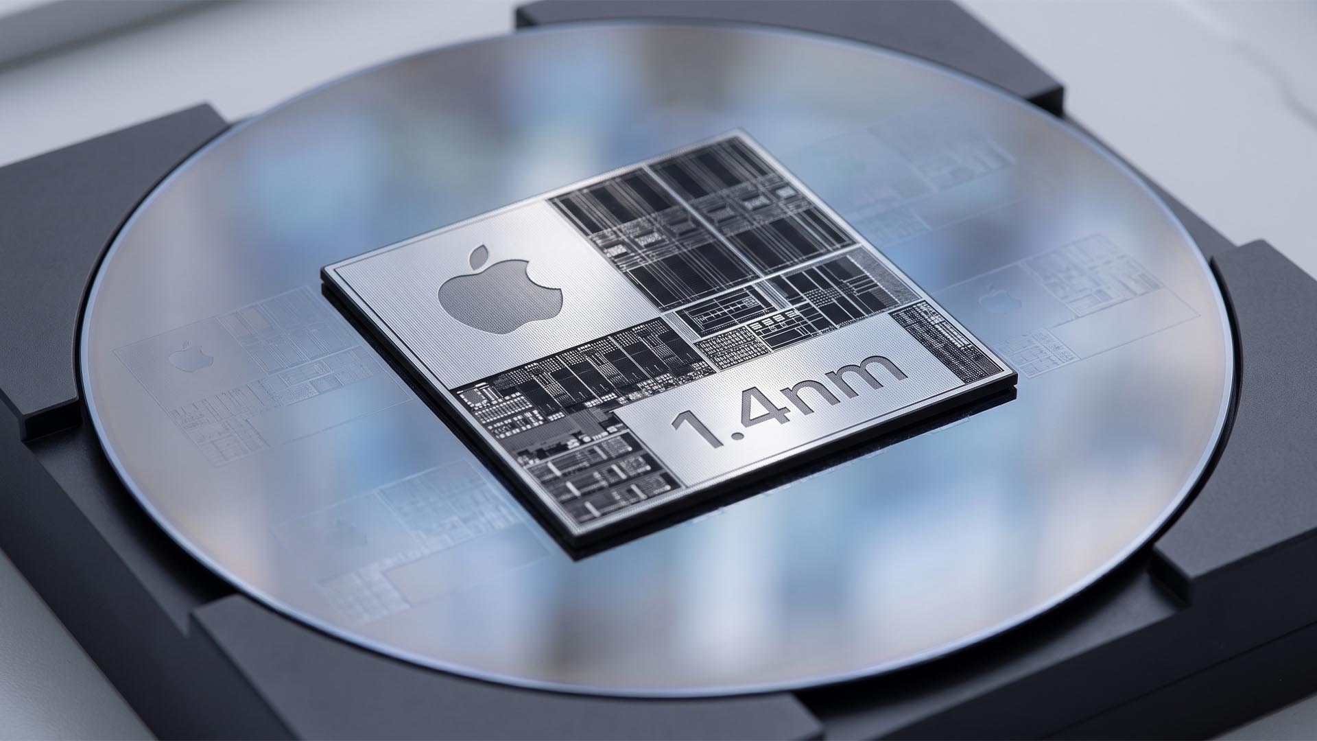
Samsung Resumes 1.4nm Process Development for Apple
💡Apple's potential move to 1.4nm signals the next frontier in AI chip efficiency and foundry competition.
⚡ 30-Second TL;DR
What Changed
Samsung shifted focus from 2nm yield optimization to accelerating 1.4nm development.
Why It Matters
The potential adoption of Samsung's 1.4nm node by Apple could diversify the high-end foundry market, currently dominated by TSMC. This competition is crucial for scaling future AI hardware infrastructure.
What To Do Next
Monitor foundry roadmap updates from Samsung and TSMC to adjust your hardware deployment strategy for large-scale AI training clusters.
🧠 Deep Insight
AI-generated analysis for this event.
🔑 Enhanced Key Takeaways
- •Samsung's 1.4nm process, internally referred to as SF1.4, utilizes an evolved Gate-All-Around (GAA) transistor architecture designed to improve power efficiency by approximately 15-20% over 2nm nodes.
- •The pivot to 1.4nm is part of Samsung Foundry's 'Samsung Advanced Foundry Ecosystem' (SAFE) initiative, which aims to integrate AI-specific IP blocks directly into the design phase to reduce time-to-market for high-performance computing (HPC) clients.
- •Industry reports indicate that Samsung is implementing a new 'Backside Power Delivery Network' (BSPDN) technology at the 1.4nm node to mitigate voltage droop and signal interference in dense AI chip layouts.
- •Apple's interest in Samsung's 1.4nm node is reportedly a diversification strategy to reduce reliance on TSMC's capacity, which is currently heavily booked for Apple's own A-series and M-series silicon.
- •Samsung has increased capital expenditure in its Pyeongtaek P4 and P5 fabrication facilities specifically to accommodate the cleanroom requirements for 1.4nm EUV (Extreme Ultraviolet) lithography equipment.
📊 Competitor Analysis▸ Show
| Feature | Samsung (1.4nm) | TSMC (1.4nm/A14) | Intel (14A) |
|---|---|---|---|
| Architecture | GAA (3rd Gen) | FinFlex/GAA (Nanosheet) | RibbonFET (GAA) |
| Targeted Launch | 2029 | 2027-2028 | 2027 |
| Primary Focus | AI/HPC Efficiency | High-Volume Mobile/AI | Foundry Services/HPC |
🛠️ Technical Deep Dive
- Transition from 2nm (SF2) to 1.4nm (SF1.4) involves scaling the nanosheet width to optimize drive current.
- Integration of High-NA EUV lithography is required to achieve the resolution necessary for 1.4nm feature sizes.
- Utilization of multi-bridge channel FET (MBCFET) technology to enhance electrostatic control over the channel.
- Implementation of advanced materials for contact resistance reduction to maintain performance at smaller pitches.
🔮 Future ImplicationsAI analysis grounded in cited sources
⏳ Timeline
Weekly AI Recap
Read this week's curated digest of top AI events →
👉Related Updates


AI-curated news aggregator. All content rights belong to original publishers.
Original source: cnBeta (Full RSS) ↗