Samsung Q2 Earnings Preview Signals Global Chip Market Trends
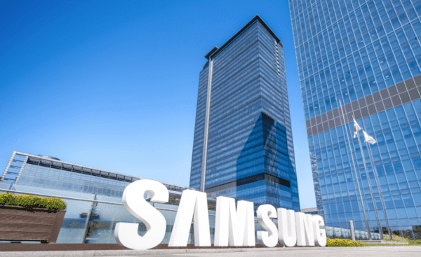
💡Samsung's massive profit surge confirms the explosive demand for memory chips powering global AI infrastructure.
⚡ 30-Second TL;DR
What Changed
Projected Q2 operating profit of 84.3 trillion KRW.
Why It Matters
Samsung's performance provides critical validation for the sustainability of the current AI hardware investment cycle.
What To Do Next
Monitor Samsung's earnings call for insights into HBM supply chain capacity, which impacts GPU availability for AI clusters.
Key Points
- •Projected Q2 operating profit of 84.3 trillion KRW.
- •Revenue expected to surge 127% to a record 169 trillion KRW.
- •Performance reflects the massive demand for memory chips in AI infrastructure.
- •Acts as a bellwether for the broader global semiconductor market.
🧠 Deep Insight
AI-generated analysis for this event — not the original article.
🔑 Enhanced Key Takeaways
- •Samsung's HBM3E (High Bandwidth Memory) production ramp-up has been a critical factor in meeting supply contracts for major AI accelerator manufacturers.
- •The surge in profitability is heavily supported by a recovery in NAND flash pricing, which had previously suffered from a prolonged inventory glut.
- •Samsung has increased its capital expenditure (CapEx) allocation toward advanced packaging technologies, specifically targeting 2.5D and 3D stacking solutions for AI chips.
- •The company's foundry division has begun to see improved yield rates for its 3nm Gate-All-Around (GAA) process, attracting new high-performance computing (HPC) clients.
- •Geopolitical trade restrictions and supply chain diversification strategies have forced Samsung to localize more of its backend assembly and testing (OSAT) operations.
📊 Competitor Analysis▸ Show
| Feature | Samsung Electronics | SK Hynix | Micron Technology |
|---|---|---|---|
| HBM Market Position | Strong (Scaling HBM3E) | Leader (Primary AI Supplier) | Challenger (HBM3E focus) |
| Foundry Capability | Full-stack (Logic + Memory) | Memory-focused | Memory-focused |
| Process Node | 3nm GAA (Mass Production) | N/A (Memory focus) | N/A (Memory focus) |
| Primary AI Strategy | Turnkey AI Solutions | HBM Dominance | High-density DRAM/NAND |
🛠️ Technical Deep Dive
- HBM3E Architecture: Utilizes 12-layer and 16-layer TSV (Throughput Silicon Via) stacking to achieve bandwidths exceeding 1.2 TB/s per stack.
- 3nm GAA (Gate-All-Around) Process: Implements Multi-Bridge-Channel FET (MBCFET) architecture to reduce power consumption by 45% and increase performance by 23% compared to FinFET.
- Advanced Packaging: Integration of I-Cube (2.5D) and X-Cube (3D) technologies to facilitate heterogeneous integration of logic and memory dies.
- NAND Flash: Transition to 9th and 10th generation V-NAND with increased layer counts to improve bit density and read/write speeds for AI data centers.
🔮 Future ImplicationsAI analysis grounded in cited sources
⏳ Timeline
Weekly AI Recap
Read this week's curated digest of top AI events →
👉Related Updates


AI-curated news aggregator. All content rights belong to original publishers.
Original source: cnBeta (Full RSS) ↗
This is a summary, not the original. Read the source, or get the weekly briefing.
Weekly AI briefing
One email a week. Unsubscribe anytime.