Samsung Overhauls HBM4E Power Net for Low Defects

💡Samsung fixes HBM4E defects, explores GPU decoupling—vital for reliable AI hardware.
⚡ 30-Second TL;DR
What Changed
Restructured power network drastically lowers HBM4E defect rates
Why It Matters
Improves reliability of AI accelerators, potentially enabling innovative decoupled HBM-GPU designs that enhance flexibility and cooling in data centers.
What To Do Next
Contact Samsung for HBM4E evaluation kits to test power efficiency in prototypes.
🧠 Deep Insight
Web-grounded analysis with 5 cited sources.
🔑 Enhanced Key Takeaways
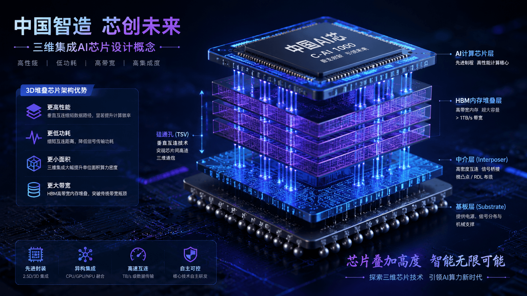
- •Samsung's HBM4E power delivery network (PDN) redesign segments the large MET4 power block into four smaller sections and redistributes upper-layer wiring for more direct routing, reducing metal circuit defects by 97% and IR drop by 41% compared to HBM4[1].
- •HBM4 features a 4nm logic base die, doubles I/O pins to 2,048 from HBM3E's 1,024, and initially offers 12-layer stacks with 24-36 GB capacity, expanding to 16-Hi 48 GB stacks[2][3].
- •The redesign addresses increased power bumps from 13,682 in HBM4 to 14,457 in HBM4E, which raised current density and resistance in denser wiring[1].
🛠️ Technical Deep Dive
- •Power bumps increase from 13,682 in HBM4 to 14,457 in HBM4E, necessitating thinner, denser wiring that elevates current density, resistance, and IR drop[1].
- •Original HBM design uses centralized honeycomb-like MET4 blocks near the interposer with narrowing upper-layer paths, creating power routing bottlenecks[1].
- •PDN overhaul divides MET4 block into four segments, segments upper layers, and optimizes routing paths to minimize detours and congestion[1].
- •HBM4 employs low-voltage TSV technology and PDN optimization for 40% power efficiency gain, 10% better thermal resistance, and 30% improved heat dissipation over HBM3E[2][3].
- •HBM4 uses 4nm logic base die with advanced 3D stacking to support doubled I/O (2,048 pins) while managing thermal and power challenges[2][3].
🔮 Future ImplicationsAI analysis grounded in cited sources
⏳ Timeline
📎 Sources (5)
Factual claims are grounded in the sources below. Forward-looking analysis is AI-generated interpretation.
- trendforce.com — News Samsung Reportedly Targets Hbm4e Power Bottleneck with Structural Overhaul Slashes Defects 97
- news.samsung.com — Samsung Ships Industry First Commercial Hbm4 with Ultimate Performance for AI Computing
- igorslab.de — Samsung Begins Mass Production of Hbm4 with Up to 13 Gbps and 48 Gb Per Stack
- sammyfans.com — Samsung Confirms Hbm4e for 2026 Custom Hbm in 2027
- techxplore.com — 2026 02 Samsung Mass Production Gen AI
Weekly AI Recap
Read this week's curated digest of top AI events →
👉Related Updates
AI-curated news aggregator. All content rights belong to original publishers.
Original source: cnBeta (Full RSS) ↗