Chinese AI Chip Makers Adopt 3D Stacking Technology
💡Learn how 3D stacking is becoming a critical workaround for AI chip performance in restricted supply environments.
⚡ 30-Second TL;DR
What Changed
3D hybrid bonding is used to overcome EUV lithography tool shortages.
Why It Matters
This shift indicates a move toward advanced packaging as a primary driver for AI hardware performance. It may lead to a new ecosystem of specialized AI accelerators that rely on architecture rather than just lithography.
What To Do Next
Evaluate how your model training pipelines can be optimized for hardware utilizing 3D-stacked memory architectures.
🧠 Deep Insight
AI-generated analysis for this event.
🔑 Enhanced Key Takeaways
- •Chinese semiconductor firms are increasingly utilizing Chiplet-based architectures (via UCIe or proprietary standards) to integrate heterogeneous dies, effectively mitigating yield issues associated with large-die monolithic designs.
- •The adoption of Through-Silicon Vias (TSV) and hybrid bonding is being accelerated by domestic equipment suppliers like AMEC and Naura Technology, which are developing localized alternatives for wafer-level packaging.
- •Major Chinese foundries are shifting focus toward 'More than Moore' strategies, prioritizing advanced packaging (2.5D/3D) to improve bandwidth and power efficiency rather than relying solely on transistor density scaling.
- •Government-backed initiatives, such as the National Integrated Circuit Industry Investment Fund (Big Fund III), are specifically earmarking capital for domestic advanced packaging and interconnect technology development.
- •The integration of High Bandwidth Memory (HBM) via 3D stacking is a primary bottleneck, with Chinese firms currently racing to develop domestic HBM3/HBM3E equivalents to pair with their AI accelerators.
📊 Competitor Analysis▸ Show
| Feature | Chinese 3D-Stacked AI Chips | NVIDIA (Blackwell/Rubin) | Intel (Gaudi/Falcon Shores) |
|---|---|---|---|
| Primary Strategy | 3D Hybrid Bonding / Chiplets | Monolithic/Advanced Packaging | Tile-based Architecture |
| Lithography | DUV (Multi-patterning) | EUV (High-NA) | EUV |
| Interconnect | Proprietary/Domestic Standards | NVLink | UCIe / EMIB |
| Performance Focus | Efficiency/Density via Stacking | Raw Compute/Scalability | Flexibility/Heterogeneous Compute |
🛠️ Technical Deep Dive
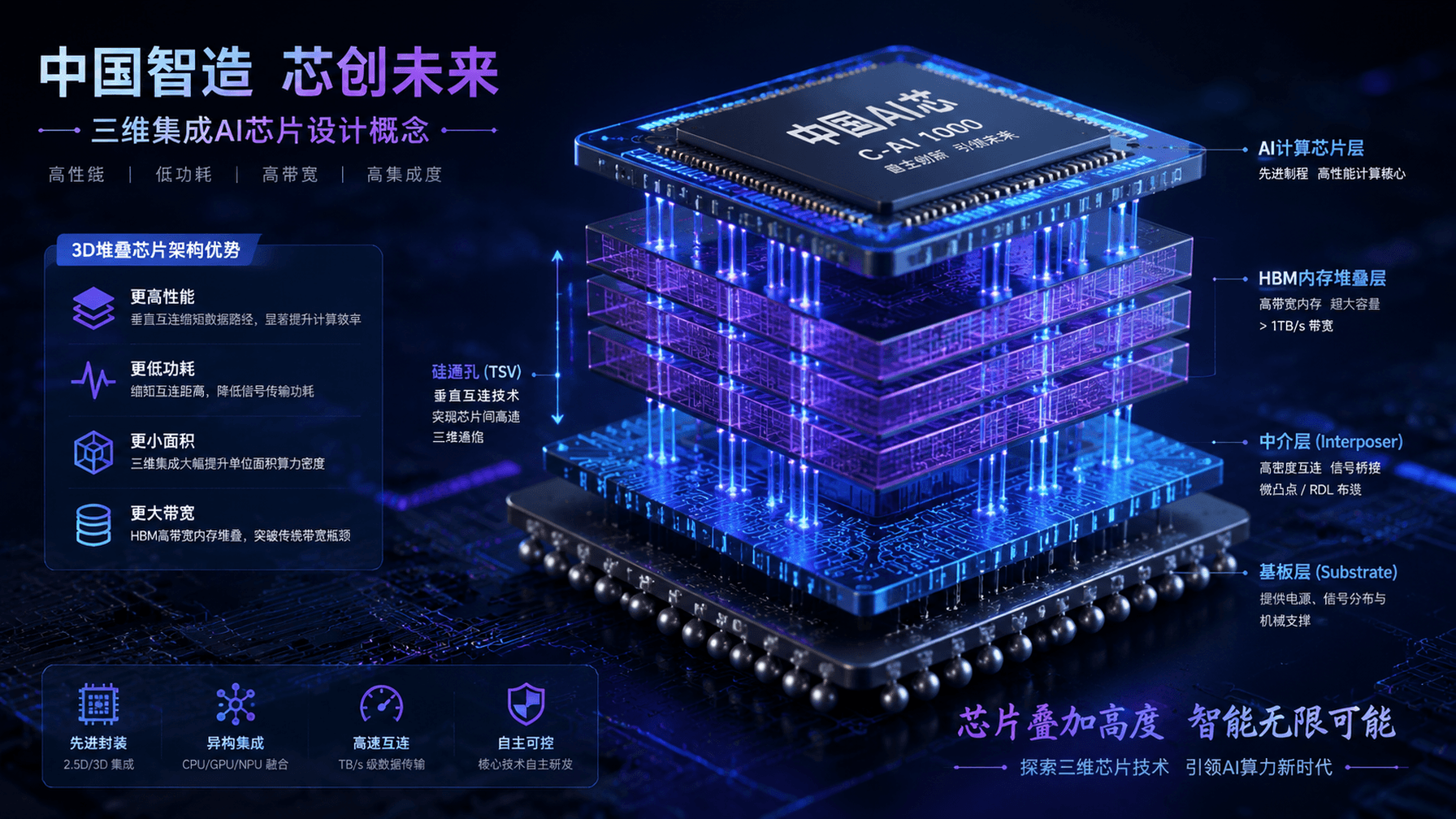
- Hybrid bonding utilizes copper-to-copper connections without solder bumps, enabling pitch sizes below 10 micrometers for higher interconnect density.
- Implementation involves wafer-to-wafer (W2W) or die-to-wafer (D2W) bonding processes to stack logic dies directly onto memory or other logic dies.
- Thermal management in 3D stacks is addressed through micro-fluidic cooling or advanced thermal interface materials (TIM) to manage the increased heat flux density of stacked layers.
- Use of TSVs (Through-Silicon Vias) allows for vertical electrical connections through the silicon substrate, reducing signal latency compared to traditional wire bonding.
🔮 Future ImplicationsAI analysis grounded in cited sources
⏳ Timeline
Weekly AI Recap
Read this week's curated digest of top AI events →
👉Related Updates

AI-curated news aggregator. All content rights belong to original publishers.
Original source: Pandaily ↗