Samsung Maps HBM’s Path to Processor-Stacked Memory
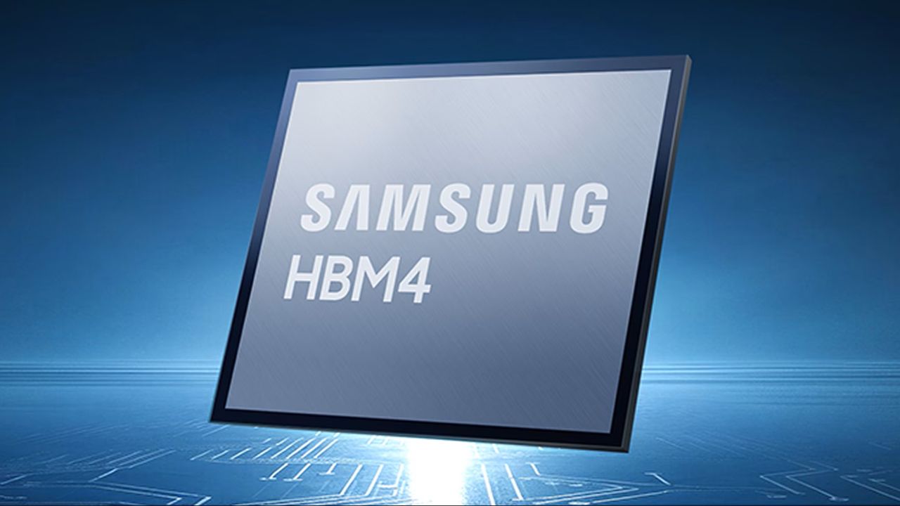
💡Samsung’s zHBM roadmap could redefine how AI accelerators place compute and memory.
⚡ 30-Second TL;DR
What Changed
Samsung presented a three-phase roadmap for increasingly compute-capable HBM.
Why It Matters
If delivered, zHBM could reduce data movement between processors and memory, a major bottleneck in AI workloads. It may also reshape accelerator packaging and memory architecture decisions for future data centers.
What To Do Next
Assess your next AI accelerator design against Samsung’s zHBM direction, focusing on memory bandwidth, thermal limits, and advanced-packaging requirements.
Key Points
- •Samsung presented a three-phase roadmap for increasingly compute-capable HBM.
- •The plan moves more logic into the HBM base die over successive phases.
- •The final zHBM design places DRAM directly on top of the processor.
🧠 Deep Insight
Background and context from public sources — not the original article. 7 sources cited.
🔑 Enhanced Key Takeaways
- •Samsung is utilizing a 4nm logic process for the HBM4 base die, transforming it from a passive interface into an active compute-capable component.
- •The zHBM architecture eliminates the need for traditional 2.5D interposers by employing wafer-on-wafer integration and hybrid copper bonding.
- •Samsung projects zHBM will achieve a 90% reduction in thermal resistance compared to current HBM standards, supported by new 'heat pipe block' cooling designs.
- •The company's vertical integration strategy leverages internal foundry and packaging capabilities to bypass the coordination delays faced by competitors relying on external partnerships.
- •Samsung introduced the V10-BV NAND architecture, which uses wafer bonding to attach a logic die to a 400-plus-layer stack, increasing density by 58% over the V9 generation.
📊 Competitor Analysis▸ Show
| Feature | Samsung zHBM | Competitors (SK Hynix/Micron) |
|---|---|---|
| Integration | Vertical 3D Stack (Wafer-on-Wafer) | Primarily 2.5D Interposer/CoWoS |
| Base Die Logic | 4nm Active Logic | Limited/Passive Base Die |
| Thermal Management | Integrated Heat Pipe/Chimney | Standard Heat Spreader |
| Ecosystem Model | Fully In-house (Foundry + Memory) | Partnership-dependent (Foundry + Memory) |
🛠️ Technical Deep Dive
- Architecture: Vertical 3D stacking of DRAM directly onto AI accelerators using hybrid copper bonding.
- Interface: Projected 8x performance increase over HBM5 standards.
- Density: Projected 10x increase in memory density compared to current HBM generations.
- Efficiency: 3x improvement in energy efficiency through reduced physical data path distance.
- Thermal: Implementation of chimney-style heat dissipation structures to manage localized hot spots in high-density stacks.
🔮 Future ImplicationsAI analysis grounded in cited sources
⏳ Timeline
📎 Sources (7)
Factual claims are grounded in the sources below. Forward-looking analysis is AI-generated interpretation.
Weekly AI Recap
Read this week's curated digest of top AI events →
👉Related Updates


AI-curated news aggregator. All content rights belong to original publishers.
Original source: Tom's Hardware ↗
This is a summary, not the original. Read the source, or get the weekly briefing.
Weekly AI briefing
One email a week. Unsubscribe anytime.