Samsung Foundry Raises Chip Prices Up to 15%
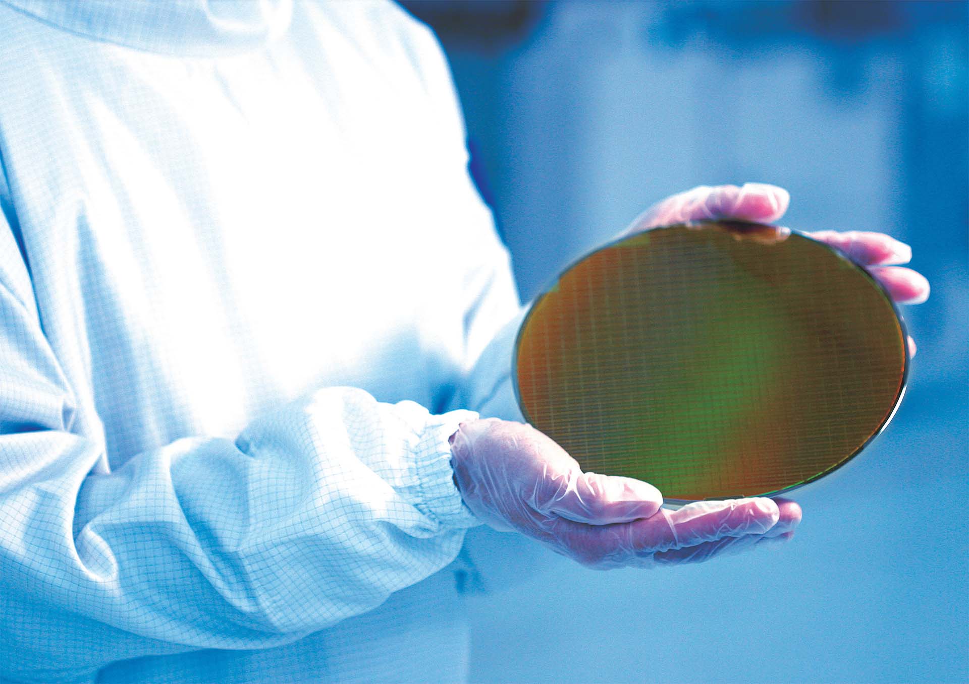
💡Rising Samsung Foundry prices could directly change the economics of AI chip development.
⚡ 30-Second TL;DR
What Changed
SF4 4nm foundry prices increased about 10%–15% for US and Chinese customers.
Why It Matters
Higher foundry prices could increase the cost of AI accelerators, edge devices, and other silicon products built on mature advanced nodes. AI startups and hardware teams may need to revisit wafer-cost assumptions, margins, and supplier diversification plans.
What To Do Next
Update your AI hardware bill of materials with 10%–15% higher SF4/SF5 wafer-cost scenarios and request refreshed quotes from Samsung Foundry and alternative suppliers.
Key Points
- •SF4 4nm foundry prices increased about 10%–15% for US and Chinese customers.
- •Taiwanese customers reportedly faced a smaller SF4 price increase of approximately 5%–10%.
- •SF5 5nm wafer prices also rose by 10%–15% amid stronger demand.
🧠 Deep Insight
Web-grounded analysis with 35 cited sources.
🔑 Enhanced Key Takeaways
- •The price increases by Samsung Foundry also extend to its older 8nm node, which saw a nearly 10% hike in July 2026.
- •The primary driver for these price adjustments is the surging global demand for AI chips, which has led to a significant tightening of capacity across the semiconductor industry, particularly for leading-edge process nodes.
- •Chinese customers are reportedly accepting the steepest price increases, largely due to U.S. export restrictions on advanced chipmaking equipment, which limits their alternative foundry options and increases their reliance on available capacity.
- •Samsung's foundry division has been operating at a loss since 2022, but these recent price hikes, combined with an influx of high-profile contracts, are projected to make the unit profitable as early as next year.
- •Competitor TSMC, the market leader, has also announced price increases of 5% to 10% across all sub-5nm nodes starting in January 2026, with some services potentially rising by around 25% in 2027, indicating a broader industry trend of rising foundry costs.
📊 Competitor Analysis▸ Show
| Foundry | Key Process Nodes (Advanced) | Market Share (Q1 2026) | Pricing (Avg. Wafer Cost) | Key Features/Notes |
|---|---|---|---|---|
| Samsung Foundry | SF4 (4nm), SF5 (5nm), SF3 (3nm GAA), SF2 (2nm GAA) | ~7% | 5nm: ~$13,000, 3nm (3GAE): ~$15,000 | SF4/SF5 use FinFET & EUV; SF3/SF2 use Gate-All-Around (GAA) MBCFET; SF4X (HPC variant) offers +10% perf, -23% power vs. standard SF4 |
| TSMC | N5 (5nm), N4 (4nm), N3 (3nm), N2 (2nm) | ~70-73% | 5nm: ~$18,500, 3nm (N3/N3E): ~$19,500, 2nm: ~$30,000 (est. H2 2025) | Dominant market leader; N5 offers 1.8x density of N7; capacity largely booked by AI orders; also raising prices (5-10% for sub-5nm in 2026, up to 25% in 2027) |
| Intel Foundry Services (IFS) | Intel 4 (internal), Intel 3 (foundry focus), 18A (1.8nm) | Not in top 10 | N/A (struggling to compete on price/yield) | Intel 4 targeted for internal compute tiles; Intel 3 is the focus for IFS; 18A aims for 3nm-equivalent density with GAAFET (RibbonFET) |
🛠️ Technical Deep Dive
- SF4 (4nm): Entered mass production in 2021, primarily for mobile applications (SF4E). It utilizes FinFET transistor architecture and Extreme Ultraviolet (EUV) lithography.
- SF4X (4nm HPC variant): This specialized version for High-Performance Computing (HPC) offers a 10% performance boost and 23% power reduction compared to the standard SF4. These improvements are achieved through advanced source/drain (SD) stress engineering, Transistor-level Design-Technology Co-Optimization (T-DTCO), and an optimized Middle-of-Line (MOL) scheme. SF4X also supports Ultra-Low-Vt (ULVT) devices, high-speed SRAM, and guarantees high Vdd (supply voltage) operation.
- SF5 (5nm): Also entered mass production in 2021, designed to enable HPC systems with enhanced performance and reduced power consumption. Built on FinFET technology with EUV lithography, it provides up to a 25% increase in logic area efficiency, 20% lower power consumption, or 10% higher performance compared to its 7nm predecessor.
- SF3 (3nm): Samsung's first 3nm process, SF3E, began mass production in 2022. It is notable for being the first to leverage Gate-All-Around (GAA) architecture with advanced nanosheet channels, which Samsung refers to as Multi-Bridge Channel FETs (MBCFETs). This transition from FinFET to GAAFET offers significant improvements in power, performance, and area (PPA) compared to 5nm, with a reported 1.23x performance increase or 45% power decrease, and a 16% area reduction.
- SF2 (2nm): Samsung's second-generation MBCFET(GAA)-based node, SF2, began mass production in 2025, targeting next-generation mobile, HPC, AI, and automotive applications with enhanced stability and higher performance.
🔮 Future ImplicationsAI analysis grounded in cited sources
⏳ Timeline
📎 Sources (35)
Factual claims are grounded in the sources below. Forward-looking analysis is AI-generated interpretation.
- thenextweb.com
- techpowerup.com
- tomshardware.com
- techi.com
- techpowerup.com
- mk.co.kr
- reddit.com
- sammyfans.com
- sammyguru.com
- cryptonomist.ch
- biggo.com
- trendforce.com
- siliconanalysts.com
- substack.com
- telecomlead.com
- substack.com
- semiwiki.com
- counterpointresearch.com
- siliconanalysts.com
- samsung.com
- wccftech.com
- techpowerup.com
- tomshardware.com
- cadence.com
- samsung.com
- fandom.com
- patentpc.com
- semiwiki.com
- namu.wiki
- samsung.com
- samsung.com
- biggo.com
- forbes.com
- semiwiki.com
- wikipedia.org
Weekly AI Recap
Read this week's curated digest of top AI events →
👉Related Updates
AI-curated news aggregator. All content rights belong to original publishers.
Original source: cnBeta (Full RSS) ↗
Weekly AI briefing
One email a week. Unsubscribe anytime.