Samsung First Produces 4F² DRAM
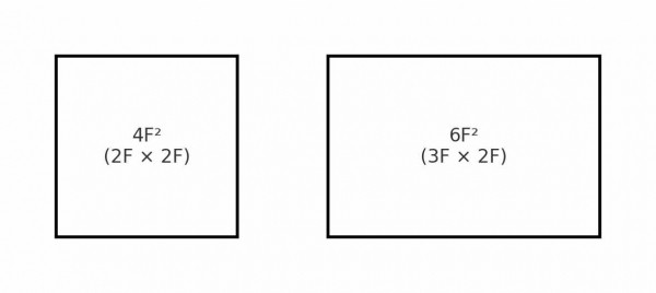
💡Samsung's 4F² DRAM shatters density limits—vital for next-gen AI hardware scaling
⚡ 30-Second TL;DR
What Changed
World's first 4F² DRAM working wafer production by Samsung
Why It Matters
This breakthrough enables ultra-high density memory, critical for AI training clusters and data centers requiring massive bandwidth and capacity.
What To Do Next
Assess 4F² DRAM integration in upcoming Nvidia or AMD AI GPU roadmaps for memory-intensive workloads.
Key Points
- •World's first 4F² DRAM working wafer production by Samsung
- •Overcomes physical limits of traditional planar DRAM scaling
- •16Gb prototype demonstrated at ISSCC 2026 in February
🧠 Deep Insight
AI-generated analysis for this event — not the original article.
🔑 Enhanced Key Takeaways
- •The 4F² architecture utilizes a vertical channel transistor (VCT) structure, which allows for a significantly smaller cell size compared to the traditional 6F² design, effectively increasing memory density by approximately 30% for the same die size.
- •Samsung's implementation addresses the critical challenge of 'aspect ratio' in capacitor manufacturing, utilizing new high-k dielectric materials and atomic layer deposition (ALD) techniques to maintain capacitance in the drastically reduced footprint.
- •Industry analysts suggest this transition is a prerequisite for reaching sub-10nm DRAM nodes, as conventional planar scaling has hit a 'scaling wall' due to leakage currents and signal interference at smaller dimensions.
📊 Competitor Analysis▸ Show
| Feature | Samsung 4F² DRAM | Micron (Current Gen) | SK Hynix (Current Gen) |
|---|---|---|---|
| Cell Architecture | 4F² (Vertical) | 6F² (Planar/Hybrid) | 6F² (Planar/Hybrid) |
| Density Scaling | High (Industry Leader) | Moderate | Moderate |
| Commercial Status | Working Wafers (2026) | R&D Phase | R&D Phase |
🛠️ Technical Deep Dive
- Architecture: Vertical Channel Transistor (VCT) design replaces the traditional access transistor layout.
- Cell Size: Achieves 4F² footprint, the theoretical minimum for a DRAM cell, compared to the industry-standard 6F².
- Manufacturing: Employs advanced EUV (Extreme Ultraviolet) lithography to pattern the dense vertical structures.
- Material Science: Integration of proprietary high-k dielectric materials to prevent data loss (capacitance drop) in the ultra-compact cell design.
- Interconnects: Utilizes multi-layer metal wiring to manage increased signal density and reduce parasitic resistance.
🔮 Future ImplicationsAI analysis grounded in cited sources
⏳ Timeline
Weekly AI Recap
Read this week's curated digest of top AI events →
👉Related Updates
AI-curated news aggregator. All content rights belong to original publishers.
Original source: cnBeta (Full RSS) ↗
This is a summary, not the original. Read the source, or get the weekly briefing.
The weekly digest
One email a week. Unsubscribe anytime.