Samsung Delays High-NA EUV Until 2030
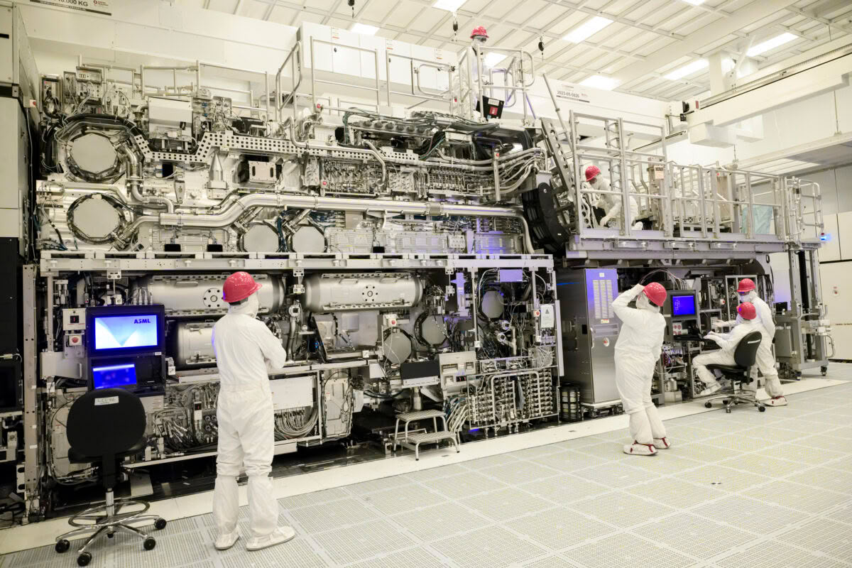
💡Samsung may delay the lithography leap that shapes future AI chip supply, cost, and performance.
⚡ 30-Second TL;DR
What Changed
Samsung Foundry is delaying a firm commitment to ASML High-NA EUV equipment.
Why It Matters
For AI companies, advanced-node foundry roadmaps influence the future availability, performance, and cost of AI accelerators. A later High-NA EUV transition could affect Samsung’s competitiveness in supplying leading-edge AI chips.
What To Do Next
Review your AI accelerator supply plan against Samsung Foundry’s 1nm and ASML High-NA EUV timeline, and identify alternative foundries for leading-edge capacity.
Key Points
- •Samsung Foundry is delaying a firm commitment to ASML High-NA EUV equipment.
- •The technology is reportedly planned for Samsung’s 1nm process development around 2030.
- •Samsung could become one of the last leading chipmakers to adopt High-NA EUV.
- •The decision may affect the timing and competitiveness of future advanced-node manufacturing.
🧠 Deep Insight
AI-generated analysis for this event.
🔑 Enhanced Key Takeaways
- •Samsung's hesitation is largely attributed to the extremely high cost of ASML's High-NA EUV machines, which are estimated to exceed $350 million per unit.
- •The company is currently prioritizing the optimization of its existing Low-NA EUV infrastructure and Gate-All-Around (GAA) transistor architecture to maximize yield before transitioning.
- •Industry analysts suggest Samsung is exploring 'multi-patterning' techniques with current Low-NA EUV tools to delay the capital expenditure required for High-NA systems.
- •Samsung's foundry division has faced significant yield challenges at advanced nodes (3nm and below), which has influenced a more conservative capital investment strategy.
- •ASML has publicly acknowledged that different chipmakers have varying timelines for High-NA adoption based on their specific product roadmaps and economic considerations.
📊 Competitor Analysis▸ Show
| Feature | Samsung Foundry | TSMC | Intel Foundry |
|---|---|---|---|
| High-NA EUV Strategy | Delayed (Targeting 2030) | Selective/Phased Adoption | Early Adopter (In-house) |
| Primary Node Focus | GAA (3nm/2nm) | FinFET/Nanosheet (2nm) | RibbonFET (18A/14A) |
| Current EUV Tech | Low-NA (0.33) | Low-NA (0.33) | High-NA (0.55) |
🛠️ Technical Deep Dive
- High-NA EUV (High Numerical Aperture Extreme Ultraviolet) lithography utilizes a 0.55 NA lens compared to the 0.33 NA of standard EUV systems.
- The increased NA allows for higher resolution patterning, enabling smaller feature sizes without the need for complex multi-patterning steps.
- High-NA systems require a larger anamorphic lens design, which necessitates a change in mask size and reticle field dimensions compared to traditional EUV.
- The transition to High-NA involves significant changes to photoresist chemistry and pellicle technology to handle the increased energy density and throughput requirements.
🔮 Future ImplicationsAI analysis grounded in cited sources
⏳ Timeline
Weekly AI Recap
Read this week's curated digest of top AI events →
👉Related Updates
在社交平台上表示,团队通过持续的技术攻坚,使该模型超越了 Nano Banana、Meta 以及 Grok 等同类竞争产品。在榜单表现上,MAI-Image-2.6 目前距离榜首 OpenAI 的 GPT-Image-2(中等版本)仅相差 45 分,同时领先第三名 Grok Imagine Image 2.0(低版本)20 分。</p><p><img src="https://static.cnbetacdn.com/article/2026/0811/e29bdb279824d65.jpg)
AI-curated news aggregator. All content rights belong to original publishers.
Original source: cnBeta (Full RSS) ↗