OpenAI’s Jalapeño Chip Challenges Blackwell
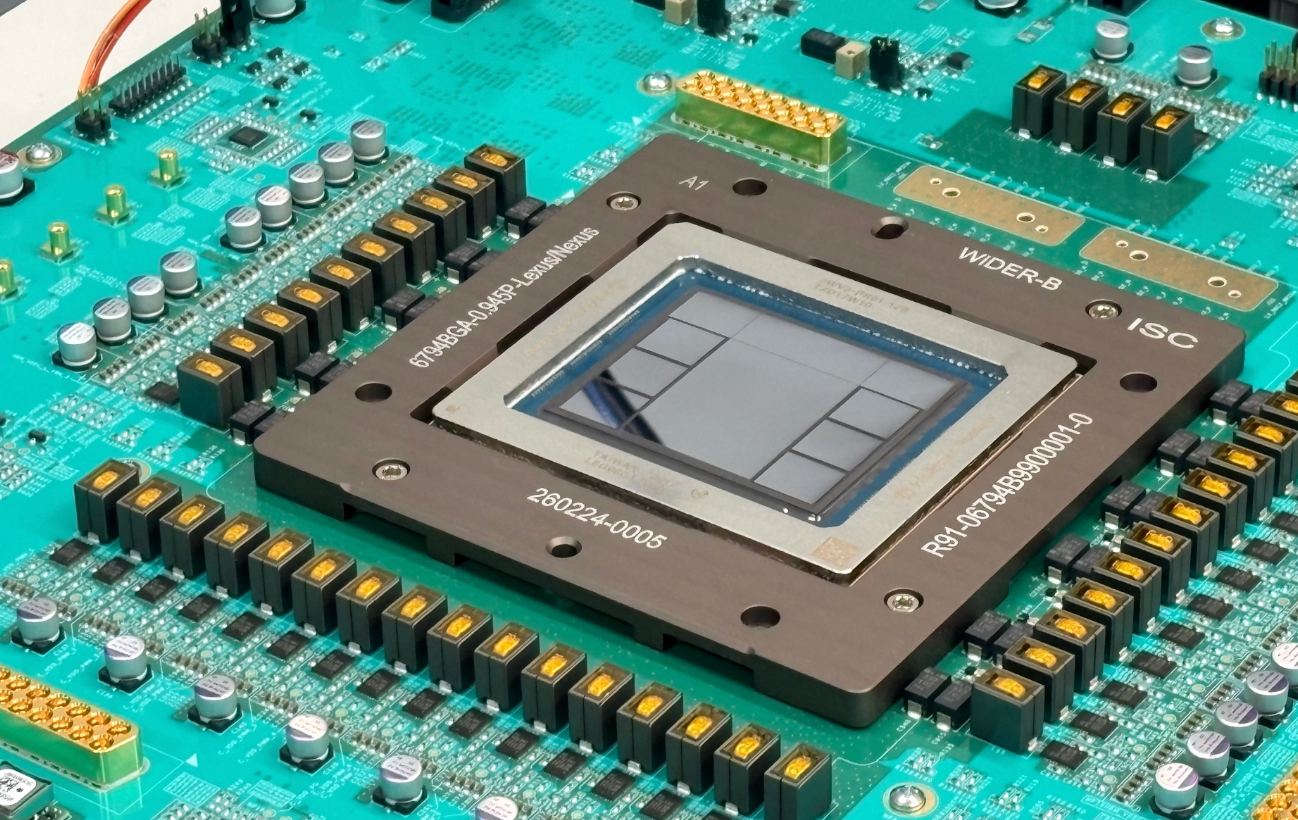
💡A model maker’s custom chip claims up to 4.9x lower-latency inference than GB300—here’s the architecture behind it.
⚡ 30-Second TL;DR
What Changed
Jalapeño reportedly delivers 1.5–1.9x Blackwell’s peak throughput per watt across GPT-OSS 120B, DeepSeek R1 670B, and Kimi K2.5 1T.
Why It Matters
If independently reproduced, Jalapeño would strengthen the case for model companies designing custom inference silicon instead of relying entirely on general-purpose GPUs. Its model-specific approach could reduce serving cost and latency, while increasing the importance of workload-aware hardware, compiler, and deployment expertise.
What To Do Next
Reproduce the InferenceX tests on your own serving stack with GPT-OSS 120B or DeepSeek R1 before using Jalapeño’s reported efficiency gains in capacity planning.
Key Points
- •Jalapeño reportedly delivers 1.5–1.9x Blackwell’s peak throughput per watt across GPT-OSS 120B, DeepSeek R1 670B, and Kimi K2.5 1T.
- •In a low-latency DeepSeek R1 test, Jalapeño reached about 700 tokens per second per user versus roughly 169 for Nvidia GB300.
- •The architecture keeps data local through compute-memory slicing and 15.4TB/s HBM4 bandwidth, reducing costly movement of model weights and KV cache.
- •OpenAI completed the first chip from initial design to tape-out in nine months and is already developing second- and third-generation versions.
- •The reported results are primarily OpenAI-provided and represent engineering-chip benchmarks rather than broad production validation.
🧠 Deep Insight
Background and context from public sources — not the original article. 16 sources cited.
🔑 Enhanced Key Takeaways
- •OpenAI utilized its own Codex model to automate and accelerate the writing of optimized kernels for the Jalapeño chip, directly challenging the dominance of Nvidia's CUDA software ecosystem.
- •The chip architecture employs a NUMA-style spatial design featuring a dedicated ultra-fast collective network specifically for performance-critical data movement, separating it from standard network-on-chip (NoC) traffic.
- •The development process was significantly expedited by using OpenAI's internal AI models to assist in the design and optimization phases, enabling a nine-month tape-out cycle.
- •Jalapeño is manufactured on a 3nm process node and operates at a 700W power rating, specifically targeting inference efficiency rather than general-purpose training workloads.
- •The hardware ecosystem includes Celestica as a key manufacturing partner alongside Broadcom, focusing on the specialized packaging required for the 15.4TB/s HBM4 bandwidth.
📊 Competitor Analysis▸ Show
| Feature | OpenAI Jalapeño | Nvidia GB300 (Blackwell) |
|---|---|---|
| Primary Focus | Inference-optimized ASIC | General-purpose AI/HPC |
| Throughput/Watt | 1.5–1.9x baseline | 1.0x (Baseline) |
| Memory Bandwidth | 15.4 TB/s (HBM4) | Industry standard (HBM3e) |
| Software Stack | Codex-optimized kernels | CUDA (Mature ecosystem) |
| Latency (DeepSeek R1) | ~700 tokens/sec/user | ~169 tokens/sec/user |
🛠️ Technical Deep Dive
- Process Node: 3nm fabrication process.
- Memory: HBM4 integration providing 15.4TB/s bandwidth.
- Power: 700W TDP per chip.
- Architecture: NUMA-style spatial compute-memory slicing.
- Interconnect: Dedicated ultra-fast collective network for critical data paths, distinct from general NoC.
🔮 Future ImplicationsAI analysis grounded in cited sources
⏳ Timeline
📎 Sources (16)
Factual claims are grounded in the sources below. Forward-looking analysis is AI-generated interpretation.
Weekly AI Recap
Read this week's curated digest of top AI events →
👉Related Updates

AI-curated news aggregator. All content rights belong to original publishers.
Original source: 极客公园 ↗
This is a summary, not the original. Read the source, or get the weekly briefing.
Weekly AI briefing
One email a week. Unsubscribe anytime.