NVIDIA Unveils NVHBM for Faster Custom AI Memory
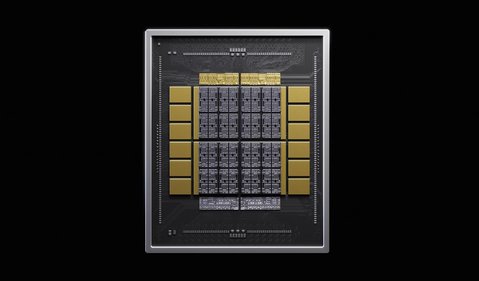
💡NVHBM could reshape AI accelerator memory bandwidth and extend NVIDIA’s ecosystem to third-party XPUs.
⚡ 30-Second TL;DR
What Changed
NVHBM moves memory-controller functions into the base die of the 3D HBM stack.
Why It Matters
If adopted at scale, NVHBM could improve memory-bound AI workloads and strengthen NVIDIA’s control over accelerator memory design. Support for third-party XPUs could also broaden NVIDIA’s hardware interconnect ecosystem.
What To Do Next
Ask your GPU and accelerator vendors whether upcoming platforms will support NVHBM and NVLink Fusion, then model the potential bandwidth impact on memory-bound inference workloads.
Key Points
- •NVHBM moves memory-controller functions into the base die of the 3D HBM stack.
- •NVIDIA plans to integrate NVHBM into future GPUs.
- •Bandwidth could be up to 30% higher than HBM4E.
- •NVLink Fusion could extend the technology to third-party XPU customers.
🧠 Deep Insight
Background and context from public sources — not the original article. 10 sources cited.
🔑 Enhanced Key Takeaways
- •NVHBM achieves a 15% reduction in HBM power consumption, providing critical thermal headroom for high-density AI compute clusters.
- •The architecture enables a 25% increase in available silicon area on the compute die by offloading memory controller functions to the HBM base die.
- •The custom physical memory interface (PHY) utilized in NVHBM reduces I/O area by up to 67% compared to standard JEDEC HBM4E specifications.
- •Amazon's Annapurna Labs has been identified as the inaugural partner for NVHBM, with integration planned for future AWS infrastructure.
- •NVIDIA is positioning NVHBM as a standardized implementation across multiple memory suppliers to lower the barrier to entry for custom silicon development.
📊 Competitor Analysis▸ Show
| Feature | NVHBM | Standard JEDEC HBM4E |
|---|---|---|
| Memory Controller Location | HBM Base Die | Compute Die |
| I/O Area Footprint | Reduced by 67% | Baseline |
| Compute Die Area Efficiency | +25% | Baseline |
| Power Consumption | -15% | Baseline |
🛠️ Technical Deep Dive
- Architecture: Shifts memory controller logic from the XPU compute die into the 3D-stacked HBM base die.
- PHY Implementation: Utilizes a proprietary physical interface design that optimizes I/O density.
- Integration: Leverages the NVLink Fusion interconnect framework to maintain coherence and high-speed data transfer between custom XPUs and the memory stack.
- Thermal Management: Reduced power draw per bit transferred allows for higher clock speeds within the same TDP envelope.
🔮 Future ImplicationsAI analysis grounded in cited sources
⏳ Timeline
📎 Sources (10)
Factual claims are grounded in the sources below. Forward-looking analysis is AI-generated interpretation.
Weekly AI Recap
Read this week's curated digest of top AI events →
👉Related Updates
AI-curated news aggregator. All content rights belong to original publishers.
Original source: cnBeta (Full RSS) ↗
This is a summary, not the original. Read the source, or get the weekly briefing.
Weekly AI briefing
One email a week. Unsubscribe anytime.