Nvidia Unveils Faster, More Efficient NVHBM
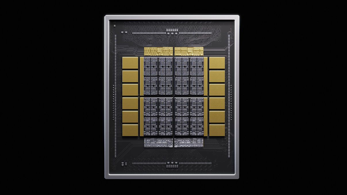
💡See how Nvidia's custom memory could reshape bandwidth and power tradeoffs for AI accelerators.
⚡ 30-Second TL;DR
What Changed
NVHBM is Nvidia's custom high-bandwidth memory implementation.
Why It Matters
For AI accelerator designers, NVHBM could improve memory-bound workload performance while reducing power budgets. Its availability through NVLink Fusion may give partner chip developers a more tightly integrated memory and interconnect path, although real-world gains will depend on implementation and workload.
What To Do Next
If you are planning a custom AI accelerator, review NVLink Fusion partner requirements and benchmark whether NVHBM's claimed bandwidth and power gains justify the platform investment.
Key Points
- •NVHBM is Nvidia's custom high-bandwidth memory implementation.
- •It promises 30% higher bandwidth than commodity HBM4e.
- •It claims 15% lower power consumption than commodity HBM4e.
- •The custom base die and PHY will be available to NVLink Fusion partners.
🧠 Deep Insight
Background and context from public sources — not the original article. 10 sources cited.
🔑 Enhanced Key Takeaways
- •NVHBM relocates the memory controller from the compute die directly into the 3D HBM stack, reclaiming up to 25% of usable silicon area on the XPU.
- •The custom NVHBM physical interface (PHY) achieves a 67% reduction in I/O area compared to JEDEC-standard HBM4e, significantly easing interposer routing complexity.
- •Amazon’s Annapurna Labs is the inaugural strategic partner, slated to integrate NVHBM into future iterations of AWS Trainium accelerators.
- •NVIDIA is standardizing the NVHBM implementation for third-party memory manufacturers to streamline the time-to-market for partners developing semi-custom AI silicon.
- •The initiative is part of a broader strategic expansion with AWS, which includes the planned deployment of 2 million additional NVIDIA GPUs across their cloud infrastructure by 2028.
📊 Competitor Analysis▸ Show
| Feature | NVHBM | Commodity HBM4e |
|---|---|---|
| Memory Controller Location | Integrated in HBM Stack | On Compute Die |
| I/O Area Footprint | Reduced by 67% | Baseline |
| Silicon Area Efficiency | +25% usable die area | Baseline |
| Bandwidth | +30% vs HBM4e | Baseline |
| Power Consumption | -15% vs HBM4e | Baseline |
🛠️ Technical Deep Dive
- Architecture: Moves memory controller logic from the XPU compute die into the 3D HBM stack.
- PHY Design: Custom physical interface optimized for reduced I/O footprint and simplified interposer routing.
- Integration: Designed as a modular building block for the NVLink Fusion ecosystem.
- Efficiency: Leverages 3D stacking to reduce signal path length and power overhead compared to standard JEDEC-compliant HBM4e implementations.
🔮 Future ImplicationsAI analysis grounded in cited sources
⏳ Timeline
📎 Sources (10)
Factual claims are grounded in the sources below. Forward-looking analysis is AI-generated interpretation.
Weekly AI Recap
Read this week's curated digest of top AI events →
👉Related Updates
AI-curated news aggregator. All content rights belong to original publishers.
Original source: Tom's Hardware ↗
This is a summary, not the original. Read the source, or get the weekly briefing.
Weekly AI briefing
One email a week. Unsubscribe anytime.