NVIDIA Unveils 1.6nm Feynman Chip
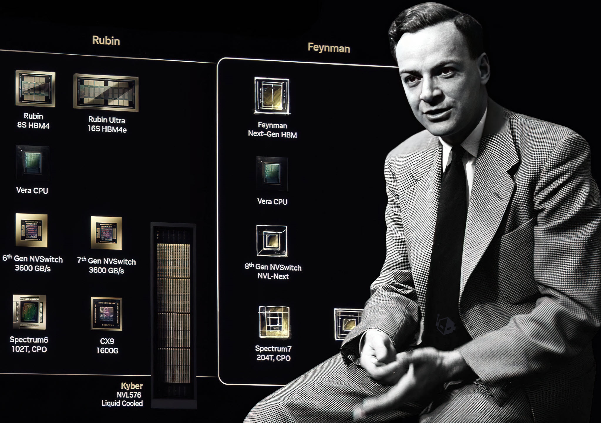
💡NVIDIA's first 1.6nm chip could double AI compute density—key for scaling models.
⚡ 30-Second TL;DR
What Changed
GTC 2026 keynote on March 15 in San Jose
Why It Matters
The 1.6nm process could enable denser transistors, slashing AI training costs and boosting inference speed for large models. NVIDIA's lead in AI infrastructure intensifies competition.
What To Do Next
Register for GTC 2026 livestream to evaluate Feynman chip specs for cluster upgrades.
Key Points
- •GTC 2026 keynote on March 15 in San Jose
- •Feynman chip as next-gen NVIDIA core product
- •World's first 1.6nm semiconductor process
- •Reported by Korean media Chosun Biz
🧠 Deep Insight
Background and context from public sources — not the original article. 6 sources cited.
🔑 Enhanced Key Takeaways
- •Nvidia will shift 25% of Feynman GPU production to Intel by 2028, using Intel's 14A process and EMIB packaging technology, while keeping the critical GPU compute die at TSMC's A16 (1.6nm) process—a historic supply chain diversification move.[2]
- •Feynman will implement next-generation HBM4e or HBM5 memory with specifications exceeding 11 Gbps speed and 3.0 TB/s bandwidth, enabling trillion-parameter scale AI model processing.[2][5]
- •The architecture leverages 3D stacking technology with vertical chiplet integration to reduce latency and increase data throughput, combined with massive arrays of high-speed SRAM for accelerating generative AI workloads.[1]
- •Feynman succeeds the current Vera Rubin line of AI accelerators and represents Nvidia's 2028 GPU generation, with potential expansion beyond data center AI into gaming and workstation markets.[2]
🛠️ Technical Deep Dive
- Process Node: TSMC A16 (1.6nm) for GPU compute die; Intel 14A or 18A for I/O die[2]
- Memory: HBM4e or HBM5 with >11 Gbps speed and 3.0 TB/s bandwidth[5]
- Architecture: Advanced chiplet design with 3D stacking and vertical integration[1]
- SRAM: Massive high-speed SRAM arrays for dataset acceleration[1]
- Packaging: EMIB (Embedded Multi-die Interconnect Bridge) for chiplet communication[2]
- I/O Die Function: Handles communication between GPU compute chiplets and external components[2]
- Capability: Designed to process trillion-parameter scale AI models[2]
🔮 Future ImplicationsAI analysis grounded in cited sources
⏳ Timeline
📎 Sources (6)
Factual claims are grounded in the sources below. Forward-looking analysis is AI-generated interpretation.
- robotdyn.com — Jensen Huang Hints at Next Gen Feynman AI Architecture Ahead of Gtc 2026
- fintool.com — Nvidia Intel Foundry Feynman 2028
- fudzilla.com — Nvidias Gtc 2026 Tease Points to Feynman Chips
- cxotoday.com — Nividia Set to Unveil a Chip That Will Surprise the World at Gtc 2026 Jensen Huang
- gurufocus.com — Nvidia Nvda Plans to Unveil Groundbreaking Chip by 2026
- finance.biggo.com — Mbxvdjwb5edqg9e4xprg
Weekly AI Recap
Read this week's curated digest of top AI events →
👉Related Updates



AI-curated news aggregator. All content rights belong to original publishers.
Original source: cnBeta (Full RSS) ↗
This is a summary, not the original. Read the source, or get the weekly briefing.
Weekly AI briefing
One email a week. Unsubscribe anytime.