🇨🇳cnBeta (Full RSS)•較早收集於 60m
NVIDIA 發布全球首款 1.6nm Feynman 晶片
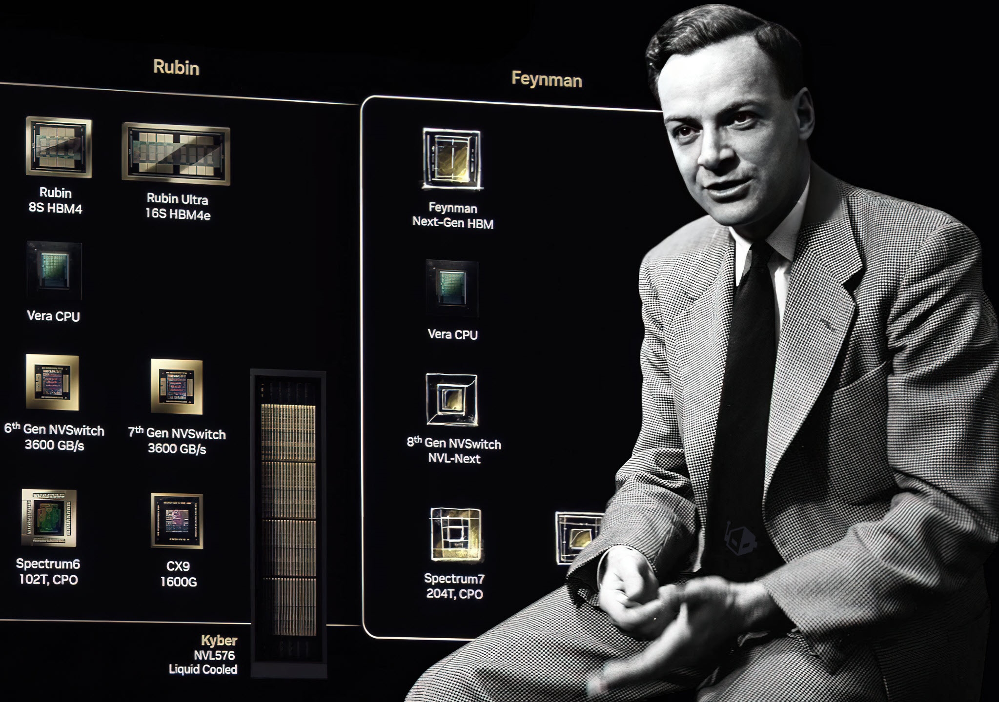
#1-6nm#chip-roadmapnvidia-feynmannvidiafeynmangtc-2026vera-rubin
💡NVIDIA's first 1.6nm chip could double AI compute density—key for scaling models.
⚡ 30-Second TL;DR
有什麼變化
GTC 2026 主題演講於 3 月 15 日聖荷西舉行
為什麼重要
1.6nm 製程可實現更高密度電晶體,降低大模型訓練成本並提升推論速度。NVIDIA 在 AI 基礎設施的主導地位加劇競爭。
下一步行動
Register for GTC 2026 livestream to evaluate Feynman chip specs for cluster upgrades.
誰應關注:Developers & AI Engineers
關鍵要點
- •GTC 2026 主題演講於 3 月 15 日聖荷西舉行
- •Feynman 晶片為 NVIDIA 下一代核心產品
- •全球首款 1.6nm 半導體製程
- •韓國媒體《朝鮮商業》報導
🧠 深度解析
背景與延伸:來自公開資料,非原文內容。引用 6 個來源。
🔑 增強重點摘要
- •Nvidia will shift 25% of Feynman GPU production to Intel by 2028, using Intel's 14A process and EMIB packaging technology, while keeping the critical GPU compute die at TSMC's A16 (1.6nm) process—a historic supply chain diversification move.[2]
- •Feynman will implement next-generation HBM4e or HBM5 memory with specifications exceeding 11 Gbps speed and 3.0 TB/s bandwidth, enabling trillion-parameter scale AI model processing.[2][5]
- •The architecture leverages 3D stacking technology with vertical chiplet integration to reduce latency and increase data throughput, combined with massive arrays of high-speed SRAM for accelerating generative AI workloads.[1]
- •Feynman succeeds the current Vera Rubin line of AI accelerators and represents Nvidia's 2028 GPU generation, with potential expansion beyond data center AI into gaming and workstation markets.[2]
🛠️ 技術深入
- Process Node: TSMC A16 (1.6nm) for GPU compute die; Intel 14A or 18A for I/O die[2]
- Memory: HBM4e or HBM5 with >11 Gbps speed and 3.0 TB/s bandwidth[5]
- Architecture: Advanced chiplet design with 3D stacking and vertical integration[1]
- SRAM: Massive high-speed SRAM arrays for dataset acceleration[1]
- Packaging: EMIB (Embedded Multi-die Interconnect Bridge) for chiplet communication[2]
- I/O Die Function: Handles communication between GPU compute chiplets and external components[2]
- Capability: Designed to process trillion-parameter scale AI models[2]
🔮 前景展望AI analysis grounded in cited sources
Intel's entry as a secondary supplier for Nvidia's flagship GPUs legitimizes Intel Foundry Services as a viable alternative to TSMC for advanced packaging.
The 25% production allocation and use of EMIB technology demonstrate confidence in Intel's manufacturing capabilities for non-core components, potentially reshaping the semiconductor supply chain hierarchy.
Feynman's trillion-parameter processing capability will enable a new class of AI models exceeding current architectural limits.
HBM4e/HBM5 memory specifications and advanced chiplet designs specifically target the memory bandwidth constraints that currently limit model scale in generative AI.
Domestic production incentives from the Trump administration are directly influencing Nvidia's supply chain strategy toward U.S. manufacturing.
Moving Feynman packaging to Intel's U.S. facilities allows Nvidia to demonstrate supply chain diversification while positioning for potential tariffs on chips manufactured abroad.
⏳ 時間線
2026-03
GTC 2026 keynote on March 15 in San Jose; Jensen Huang unveils Feynman chip architecture
2028-01
Feynman GPU production begins with 25% allocation to Intel Foundry using 14A/18A process
📎 來源 (6)
Factual claims are grounded in the sources below. Forward-looking analysis is AI-generated interpretation.
- robotdyn.com — Jensen Huang Hints at Next Gen Feynman AI Architecture Ahead of Gtc 2026
- fintool.com — Nvidia Intel Foundry Feynman 2028
- fudzilla.com — Nvidias Gtc 2026 Tease Points to Feynman Chips
- cxotoday.com — Nividia Set to Unveil a Chip That Will Surprise the World at Gtc 2026 Jensen Huang
- gurufocus.com — Nvidia Nvda Plans to Unveil Groundbreaking Chip by 2026
- finance.biggo.com — Mbxvdjwb5edqg9e4xprg
📰
AI 週報
閱讀本週精選 AI 大事摘要 →
👉相關動態


AI 策展新聞聚合。所有內容版權歸原始發布者所有。
原始來源: cnBeta (Full RSS) ↗
每週 AI 簡報
每週一封,可隨時退訂。