NVIDIA Reportedly Targets TSMC A16 for Feynman
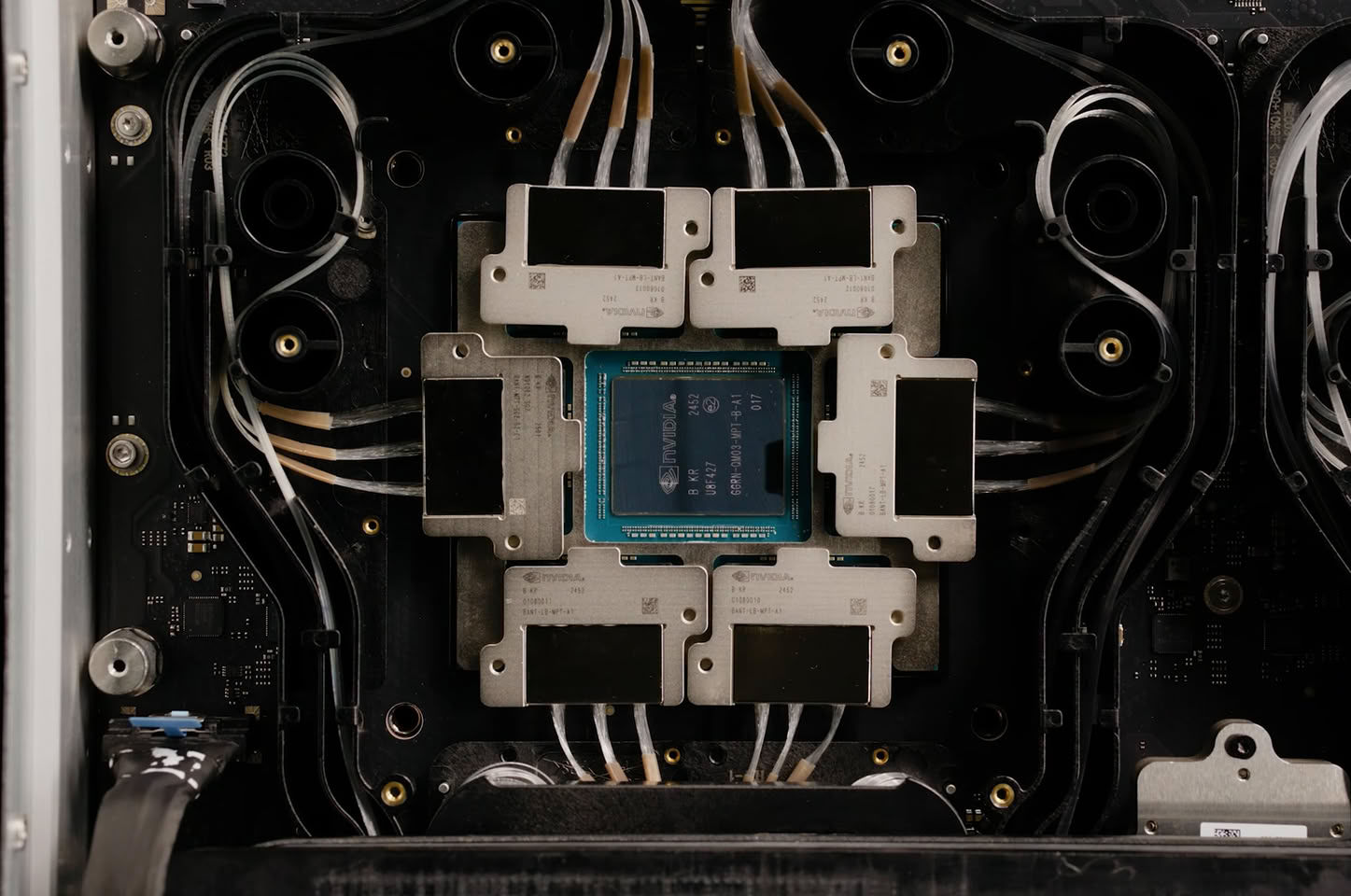
💡NVIDIA’s reported A16 shift could reshape the next generation of AI accelerator capacity planning.
⚡ 30-Second TL;DR
What Changed
Feynman is expected to succeed NVIDIA’s Rubin and Rubin Ultra GPU families.
Why It Matters
If confirmed, the A16 selection would signal NVIDIA’s pursuit of further performance and efficiency gains for future AI accelerators. It could also affect long-term capacity planning, packaging demand, and infrastructure roadmaps for AI data centers.
What To Do Next
Review your 2028 GPU capacity plan and track NVIDIA Feynman, TSMC A16, and Rubin roadmap updates before committing to long-lived accelerator infrastructure.
Key Points
- •Feynman is expected to succeed NVIDIA’s Rubin and Rubin Ultra GPU families.
- •NVIDIA reportedly plans to use TSMC’s A16 process instead of the N2 family.
- •Mass production is projected for the second half of 2028.
- •The information comes from supply-chain sources and people close to TSMC, so it remains unconfirmed.
🧠 Deep Insight
AI-generated analysis for this event.
🔑 Enhanced Key Takeaways
- •TSMC's A16 process node integrates 'Super Power Rail' (SPR) technology, which moves power delivery to the backside of the wafer to reduce IR drop and improve logic density by up to 20% compared to N2P.
- •The transition to A16 represents a strategic shift for NVIDIA, bypassing the N2P (2nm enhanced) node to prioritize the performance-per-watt gains inherent in backside power delivery.
- •Feynman is anticipated to leverage HBM4e memory technology, which is expected to be the standard for high-end AI accelerators by the 2028 timeframe.
- •Industry analysts suggest that NVIDIA's adoption of A16 is driven by the need to maintain a competitive edge in thermal management as GPU TDPs (Thermal Design Power) continue to climb toward the 1000W+ threshold.
- •The development of Feynman is occurring in parallel with NVIDIA's efforts to diversify its foundry strategy, though TSMC remains the primary partner for leading-edge nodes due to yield maturity.
📊 Competitor Analysis▸ Show
| Feature | NVIDIA Feynman (Est.) | AMD Instinct Next-Gen | Intel Gaudi/Falcon |
|---|---|---|---|
| Process Node | TSMC A16 | TSMC N2/A16 (Rumored) | Intel 18A/TSMC |
| Memory | HBM4e | HBM4/HBM4e | HBM3e/HBM4 |
| Architecture | Blackwell Successor | CDNA 4/5 | Falcon Shores |
| Market Focus | Hyperscale AI/LLM | HPC/AI Training | Enterprise AI |
🛠️ Technical Deep Dive
- A16 Process: Utilizes Backside Power Delivery Network (BSPDN) to decouple power and signal routing, significantly reducing interconnect resistance.
- Logic Density: A16 offers a claimed 1.07x to 1.10x density improvement over N2P, allowing for more complex GPU compute dies within the same reticle limit.
- Power Efficiency: The Super Power Rail architecture is designed to provide cleaner power delivery, essential for high-frequency operation in large-scale AI clusters.
- Interconnects: Expected to utilize advanced CoWoS (Chip-on-Wafer-on-Substrate) packaging to integrate high-bandwidth memory stacks with the compute die.
🔮 Future ImplicationsAI analysis grounded in cited sources
⏳ Timeline
Weekly AI Recap
Read this week's curated digest of top AI events →
👉Related Updates

AI-curated news aggregator. All content rights belong to original publishers.
Original source: cnBeta (Full RSS) ↗