🇨🇳cnBeta (Full RSS)•Stalecollected in 21h
Nikon Posts Worst-Ever 85B Yen Loss Warning

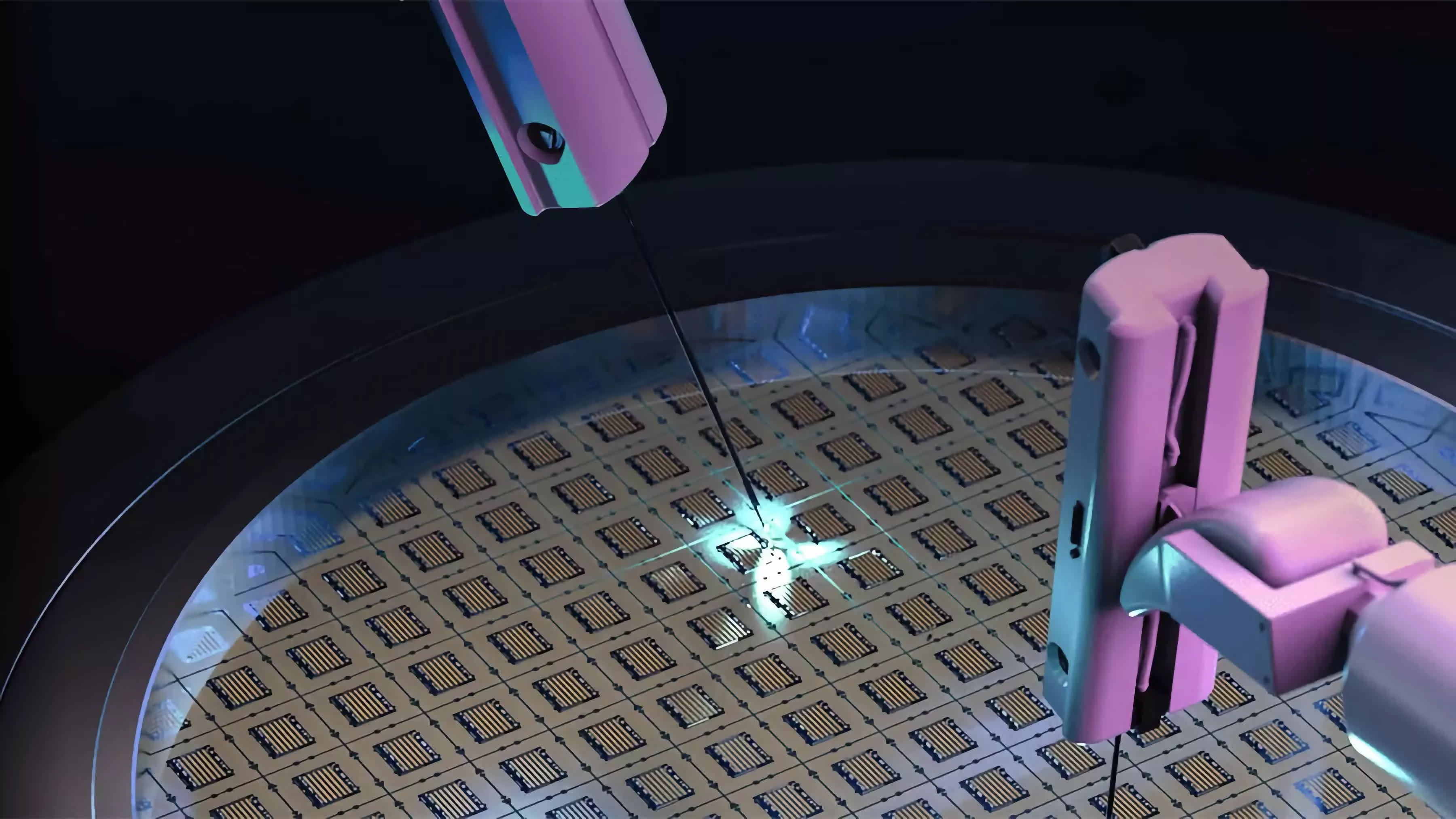
💡Nikon litho collapse risks AI chip supply chain disruptions
⚡ 30-Second TL;DR
What Changed
850 billion yen projected loss for FY2025
Why It Matters
Nikon's crisis may disrupt lithography tool supply for semiconductor fabs producing AI chips. This could lead to tighter capacity in chip manufacturing, raising costs for AI hardware. Practitioners should watch for ripple effects on GPU and accelerator production.
What To Do Next
Review your AI hardware supply chain for Nikon tool dependencies and explore ASML alternatives.
Who should care:Enterprise & Security Teams
Key Points
- •850 billion yen projected loss for FY2025
- •Worst financial result in 107-year history
- •Core lithography business in full retreat
- •Signals survival crisis for former leader
🧠 Deep Insight
AI-generated analysis for this event.
🔑 Enhanced Key Takeaways
- •The collapse is primarily attributed to Nikon's failure to transition from ArF immersion lithography to EUV (Extreme Ultraviolet) technology, leaving them unable to compete with ASML for sub-7nm node manufacturing.
- •Nikon's Precision Equipment segment, which historically provided the bulk of its revenue, has seen its market share in the semiconductor lithography sector drop to single digits as major foundries shifted exclusively to EUV-based processes.
- •The company is currently exploring a massive restructuring plan that includes the potential divestment of its semiconductor equipment division and a pivot toward industrial metrology and specialized optical components to preserve cash flow.
📊 Competitor Analysis▸ Show
| Feature | Nikon (Lithography) | ASML (Lithography) | Canon (Lithography) |
|---|---|---|---|
| Primary Tech | ArF Immersion / i-line | EUV / DUV | Nanoimprint / i-line |
| Market Position | Legacy/Niche | Dominant (EUV) | Niche/Specialized |
| Sub-7nm Capability | None | Industry Standard | Limited (Nanoimprint) |
🔮 Future ImplicationsAI analysis grounded in cited sources
Nikon will exit the high-end semiconductor lithography market by 2027.
The scale of the 850 billion yen loss suggests the company can no longer sustain the R&D expenditure required to catch up to EUV technology.
Nikon's imaging division will be spun off as an independent entity.
To survive the liquidity crisis, the company is likely to separate its profitable but capital-intensive consumer camera business from the failing industrial segments.
⏳ Timeline
1917-07
Nikon established as Nippon Kogaku Kogyo K.K.
1980-01
Nikon enters the semiconductor lithography market with the NSR-1010G.
2010-03
Nikon reaches peak market dominance in ArF immersion lithography systems.
2023-11
Nikon announces a strategic shift toward industrial metrology and digital manufacturing.
2025-04
Nikon reports first-quarter fiscal losses signaling the start of the current financial crisis.
📰
Weekly AI Recap
Read this week's curated digest of top AI events →
👉Related Updates

AI-curated news aggregator. All content rights belong to original publishers.
Original source: cnBeta (Full RSS) ↗