Nexperia China Shifts Entire Line to Domestic Wafers
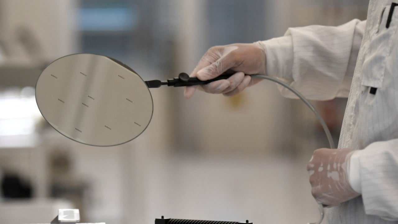
💡Nexperia’s wafer shift shows how semiconductor independence efforts could reshape AI hardware supply chains.
⚡ 30-Second TL;DR
What Changed
Nexperia China intends to transition its entire product line to a domestic 12-inch wafer foundry.
Why It Matters
A domestic wafer supply could reduce Nexperia China’s dependence on European fabrication capacity, but it may also create qualification and supply-chain transition risks. For AI hardware buyers, the development highlights how geopolitical and corporate disputes can affect semiconductor sourcing.
What To Do Next
Ask semiconductor and cloud suppliers whether Nexperia China’s wafer transition changes qualification status, lead times, or sourcing risk for your AI hardware.
Key Points
- •Nexperia China intends to transition its entire product line to a domestic 12-inch wafer foundry.
- •The unit previously sourced wafers from Nexperia’s European fabrication plants.
- •The move follows a nearly one-year dispute with the company’s European headquarters and is framed as operational independence.
🧠 Deep Insight
Background and context from public sources — not the original article. 11 sources cited.
🔑 Enhanced Key Takeaways
- •The transition was triggered by a formal cutoff of wafer shipments from the Dutch headquarters to the Chinese subsidiary in October 2025.
- •Nexperia China claims the shift to 12-inch wafers has reduced automotive chip lead times from 12–16 months down to approximately five weeks.
- •Nexperia B.V. has issued global alerts warning that it cannot verify the AEC-Q101 automotive-grade certification for components manufactured using the new domestic wafer supply.
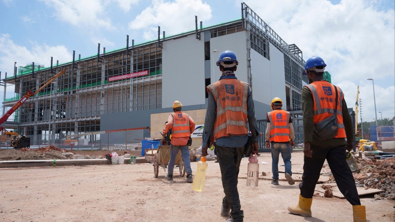
- •The Dutch headquarters is concurrently executing a $300 million expansion in Malaysia to shift 90% of its global production capacity away from China.
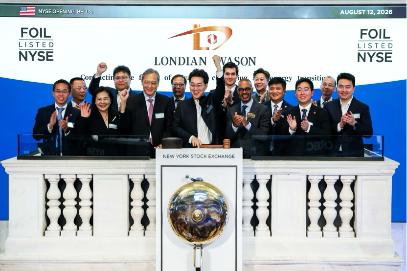
- •A Dutch court has intervened in the governance of Nexperia Holding B.V., appointing independent administrators and suspending executives affiliated with the Chinese parent company, Wingtech Technology.
📊 Competitor Analysis▸ Show
| Feature | Nexperia (China Unit) | Nexperia (Global/Dutch) |
|---|---|---|
| Wafer Size | 12-inch (Domestic) | 6/8-inch (European/Global) |
| Supply Chain | Fully Localized | Diversified (Malaysia/Europe) |
| Certification | Unverified (AEC-Q101) | Validated (AEC-Q101) |
| Lead Times | ~5 Weeks | Standard Industry Lead Times |
🛠️ Technical Deep Dive
- Transitioning product portfolio including diodes, MOSFETs, and logic integrated circuits to 12-inch wafer fabrication.
- Shift from legacy 6-inch and 8-inch wafer processes to 12-inch platforms to improve cost efficiency and surface area utilization.
- Implementation of localized R&D and independent operating systems to manage product iteration cycles of 9–12 months.
🔮 Future ImplicationsAI analysis grounded in cited sources
⏳ Timeline
📎 Sources (11)
Factual claims are grounded in the sources below. Forward-looking analysis is AI-generated interpretation.
Weekly AI Recap
Read this week's curated digest of top AI events →
👉Related Updates
AI-curated news aggregator. All content rights belong to original publishers.
Original source: SCMP Technology ↗
This is a summary, not the original. Read the source, or get the weekly briefing.
Weekly AI briefing
One email a week. Unsubscribe anytime.