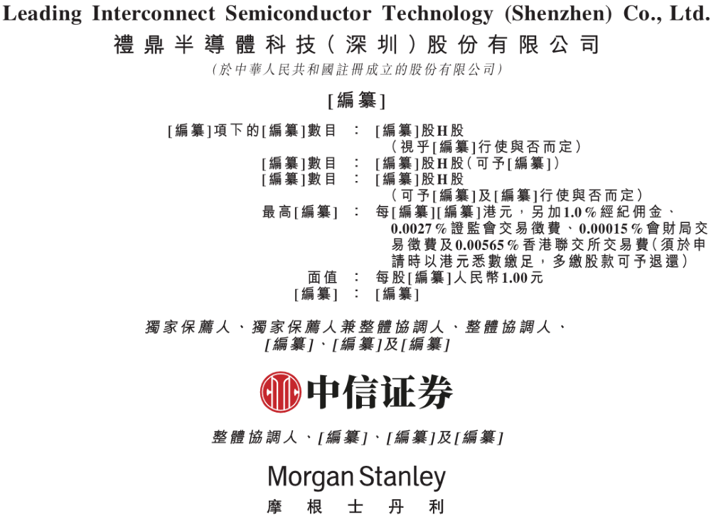
Liding Semiconductor files for IPO with 2nm tech breakthrough
💡Domestic breakthrough in 2nm-compatible IC substrates offers a new supply chain option for high-end AI hardware.
⚡ 30-Second TL;DR
What Changed
Liding Semiconductor achieved mass production capabilities for 2nm-compatible FCBGA substrates.
Why It Matters
Liding's advancement signals the increasing importance of domestic IC substrate suppliers in the global AI hardware supply chain.
What To Do Next
Evaluate Liding's substrate specifications for your hardware projects if you are sourcing components for high-performance AI chips.
Key Points
- •Liding Semiconductor achieved mass production capabilities for 2nm-compatible FCBGA substrates.
- •Revenue grew significantly, driven by AI and HPC demand, which now accounts for 25.3% of total revenue.
- •The company is the first in mainland China to mass-produce substrates for chips with 11+ chiplets.
🧠 Deep Insight
AI-generated analysis for this event — not the original article.
🔑 Enhanced Key Takeaways
- •Liding Semiconductor's IPO filing indicates a strategic shift toward domestic supply chain independence, aiming to reduce reliance on Japanese and Taiwanese substrate manufacturers like Ibiden and Unimicron.
- •The company's 2nm-compatible substrate utilizes advanced ABF (Ajinomoto Build-up Film) alternative materials, addressing critical supply chain bottlenecks for high-end AI accelerators.
- •Liding has secured long-term supply agreements with major domestic AI chip designers, signaling a transition from a component supplier to a core partner in the Chinese HPC ecosystem.
- •The IPO proceeds are earmarked for the construction of a new 'Smart Factory' in Shenzhen, which is expected to increase their high-end FCBGA production capacity by 40% by late 2027.
- •The company has successfully integrated glass-core substrate research into its R&D pipeline, positioning itself for the next generation of packaging technology beyond traditional organic substrates.
📊 Competitor Analysis▸ Show
| Feature | Liding Semiconductor | Ibiden (Japan) | Unimicron (Taiwan) |
|---|---|---|---|
| 2nm Support | Mass Production | Mass Production | Mass Production |
| Primary Market | Mainland China | Global/Tier-1 | Global/Tier-1 |
| Tech Focus | AI/HPC Chiplets | High-End CPU/GPU | High-End CPU/GPU |
| Pricing Strategy | Competitive/Domestic | Premium | Premium |
🛠️ Technical Deep Dive
- Substrate Architecture: Utilizes a multi-layer build-up process with ultra-fine pitch (less than 10μm) to support high-density interconnects required for 2nm chiplets.
- Chiplet Integration: Employs advanced thermal management materials to handle the high TDP (Thermal Design Power) of AI accelerators exceeding 700W.
- Material Innovation: Uses proprietary resin formulations to replace traditional ABF, improving signal integrity and reducing dielectric loss at high frequencies.
- Interconnect Density: Supports high-density routing for 11+ chiplet configurations, enabling complex heterogeneous integration.
🔮 Future ImplicationsAI analysis grounded in cited sources
⏳ Timeline
Weekly AI Recap
Read this week's curated digest of top AI events →
👉Related Updates


AI-curated news aggregator. All content rights belong to original publishers.
Original source: 虎嗅 ↗
This is a summary, not the original. Read the source, or get the weekly briefing.
Weekly AI briefing
One email a week. Unsubscribe anytime.