🔥36氪•Freshcollected in 2m
Lens Technology: Glass Substrate Business Faces Uncertainty

💡Understand the supply chain bottlenecks for next-gen AI chip packaging materials.
⚡ 30-Second TL;DR
What Changed
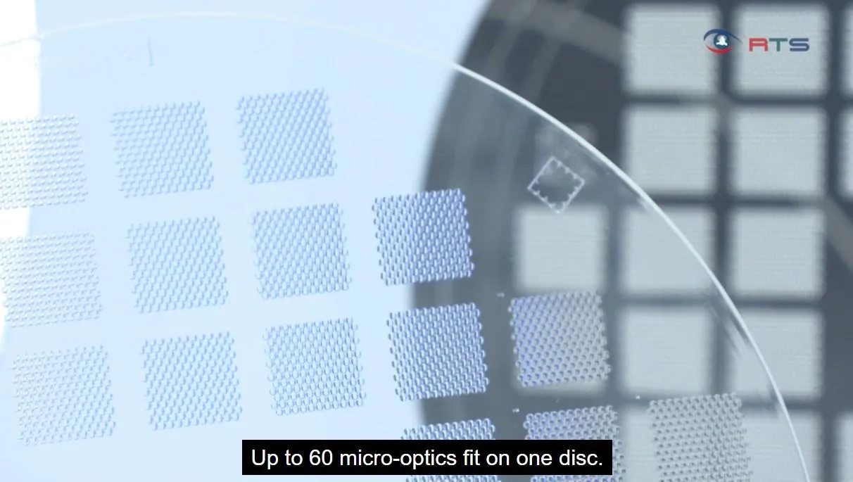
Glass substrate business currently generates zero revenue
Why It Matters
The lack of revenue in this high-tech material segment suggests that advanced packaging infrastructure for AI chips remains in a long-term R&D phase.
What To Do Next
Monitor supply chain reports on glass substrate mass production timelines to gauge AI hardware scaling.
Who should care:Founders & Product Leaders
🧠 Deep Insight
AI-generated analysis for this event.
🔑 Enhanced Key Takeaways
- •Lens Technology's glass substrate initiative is primarily targeted at next-generation semiconductor packaging and AI-driven high-performance computing (HPC) applications.
- •The company is facing significant yield rate challenges in glass-based interposer manufacturing, which is a primary factor delaying commercial revenue generation.
- •Lens Technology has been heavily investing in R&D for glass-through-via (TGV) technology to compete with traditional organic substrate materials.
- •Industry analysts note that the transition from organic to glass substrates requires a complete overhaul of existing backend semiconductor assembly and test (OSAT) equipment.
- •The company's capital expenditure (CapEx) remains high due to the acquisition of specialized laser drilling and precision etching equipment required for glass substrate processing.
📊 Competitor Analysis▸ Show
| Feature | Lens Technology | Ibiden | Schott AG | Corning |
|---|---|---|---|---|
| Focus | Glass Substrate/TGV | Organic/Glass Hybrid | Specialty Glass Material | Glass Material/Substrate |
| Market Status | Pre-revenue/R&D | Established Leader | Material Supplier | Material/Substrate R&D |
| Key Strength | Precision Manufacturing | Packaging Integration | Material Science | Glass Composition |
🛠️ Technical Deep Dive
- Glass-Through-Via (TGV) technology utilizes laser-induced deep etching to create high-density interconnects in glass panels.
- Glass substrates offer superior dimensional stability and lower signal loss compared to traditional organic substrates (ABF) at high frequencies.
- Thermal expansion coefficient (CTE) matching between glass and silicon dies is a critical technical hurdle for reliability in large-scale packaging.
- Precision surface planarization is required to achieve the sub-micron flatness necessary for advanced lithography processes on glass substrates.
🔮 Future ImplicationsAI analysis grounded in cited sources
Lens Technology will likely pivot toward strategic partnerships with major OSAT providers to share development costs.
The high capital intensity and technical complexity of glass substrate manufacturing make independent scaling financially risky for a single component supplier.
Commercial adoption of glass substrates will remain limited to niche high-end AI server chips through 2027.
Current manufacturing costs and yield challenges prevent glass substrates from replacing cost-effective organic substrates in consumer electronics.
⏳ Timeline
2023-05
Lens Technology announces strategic shift toward semiconductor packaging materials.
2024-02
Company completes pilot line installation for glass substrate R&D.
2025-09
Lens Technology reports initial testing phases for TGV-based glass interposers.
2026-06
Management issues formal disclosure regarding revenue delays in the glass substrate segment.
📰
Weekly AI Recap
Read this week's curated digest of top AI events →
👉Related Updates


AI-curated news aggregator. All content rights belong to original publishers.
Original source: 36氪 ↗