Korean Chipmakers Buzz Over HBF Memory Breakthrough
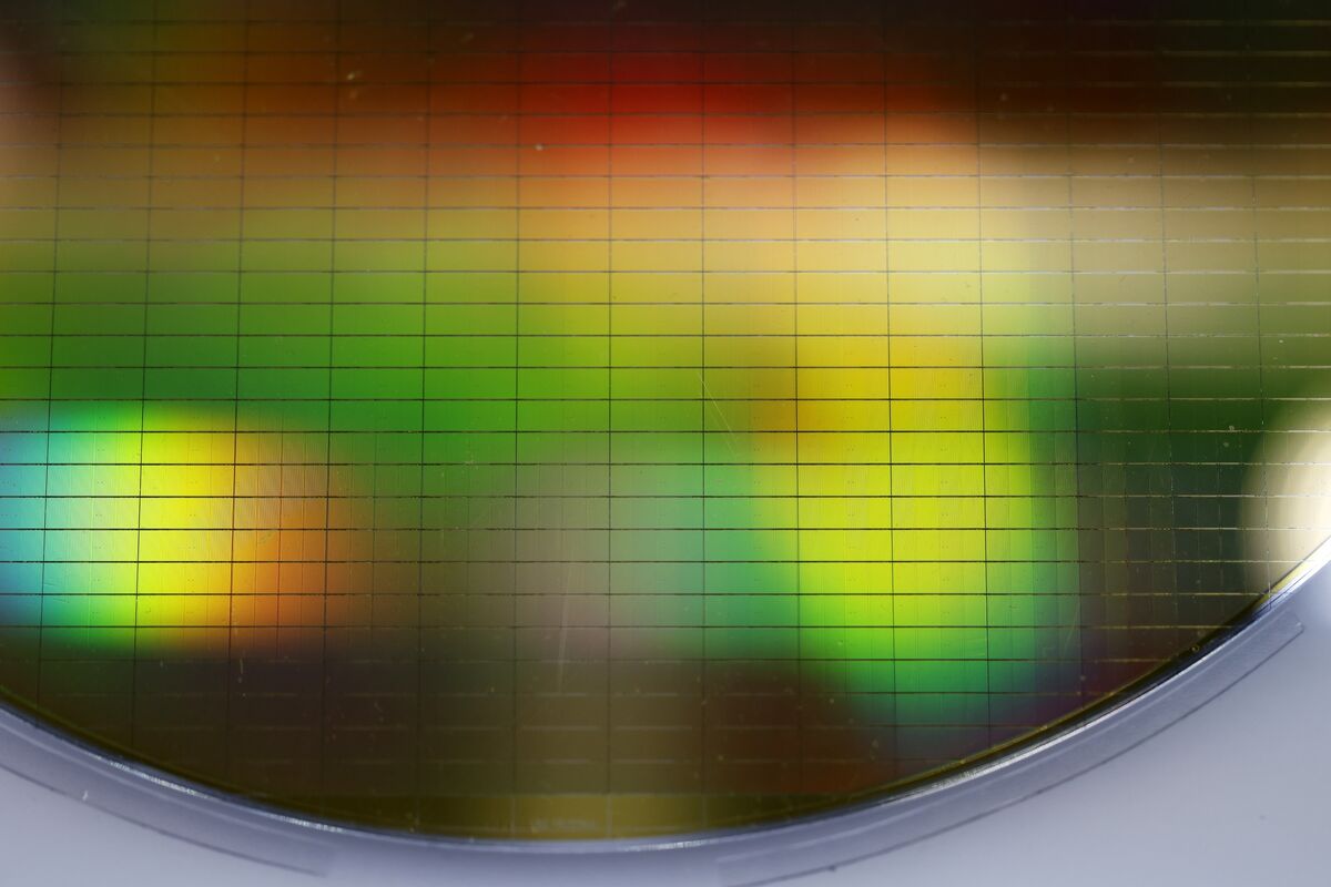
💡HBF memory breakthrough eyes AI bandwidth crunch—watch Korea's next HBM killer
⚡ 30-Second TL;DR
What Changed
Korean firms target HBF for memory advancement
Why It Matters
HBF could alleviate memory bottlenecks for AI training/inference, boosting GPU efficiency. Strengthens Korea's lead in AI infrastructure supply chain.
What To Do Next
Evaluate HBF prototypes for integration in custom AI accelerator designs.
Key Points
- •Korean firms target HBF for memory advancement
- •High-bandwidth flash generates industry buzz
- •Potential successor to HBM in AI/data centers
- •Focus on home of global memory production
🧠 Deep Insight
Background and context from public sources — not the original article. 8 sources cited.
🔑 Enhanced Key Takeaways
- •HBF employs die stacking, through-silicon vias (TSVs), and DDR synchronous signaling to achieve up to 800 GB/s aggregate bandwidth and 1.6 TiB capacity per stack[1].
- •HBF targets read-oriented workloads like LLM inference, offering 20-30% better energy efficiency at 0.48 nJ/byte with multi-way interleaving compared to conventional flash[1].
- •HBF maintains backward compatibility with existing flash pinouts and supports fallback to single-data-rate timing without new pins[1].
- •SanDisk has developed HBF to deliver performance within 2.2% of unlimited-capacity HBM while scaling capacity significantly for AI applications[8].
🛠️ Technical Deep Dive
- •Architecture: NAND flash with multi-layer die stacking (each die has hundreds of 3D NAND layers), TSVs for vertical interconnects, and HBM-style host interfaces[1][7].
- •Bandwidth: 400–800 GB/s aggregate per stack; single-channel DDR achieves 2–3× gains over SDR flash interfaces[1].
- •Capacity: ~1.6 TiB per stack, 16× larger than HBM4's ~100 GiB[1].
- •Energy: 0.48 nJ/byte at sixteen-way SLC interleaving, 20-30% reduction vs. conventional[1].
- •Interface: Multi-channel/way interleaving, DDR synchronous signaling, backward-compatible pinout and SDR fallback[1].
🔮 Future ImplicationsAI analysis grounded in cited sources
⏳ Timeline
📎 Sources (8)
Factual claims are grounded in the sources below. Forward-looking analysis is AI-generated interpretation.
- emergentmind.com — High Bandwidth Flash Hbf
- rambus.com — Hbm3 Everything You Need to Know
- microchipusa.com — Ultimate Guide to High Bandwidth Memory
- simms.co.uk — What Is Hbm High Bandwidth Memory
- en.wikipedia.org — High Bandwidth Memory
- youtube.com — Watch
- blocksandfiles.com — 1713383
- sandisk.com — Scaling Beyond the Wall Inside Sandisks High Bandwidth Flash for AI
Weekly AI Recap
Read this week's curated digest of top AI events →
👉Related Updates
AI-curated news aggregator. All content rights belong to original publishers.
Original source: Bloomberg Technology ↗
This is a summary, not the original. Read the source, or get the weekly briefing.
Weekly AI briefing
One email a week. Unsubscribe anytime.