📊Bloomberg Technology•較早收集於 33m
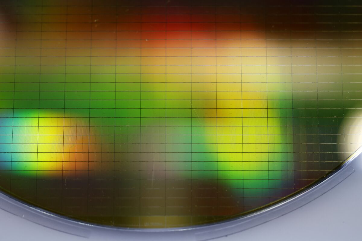
韓國記憶體廠商熱議 HBF 下一代突破
#memory-chips#high-bandwidth-flashhbfhbf
💡HBF memory breakthrough eyes AI bandwidth crunch—watch Korea's next HBM killer
⚡ 30-Second TL;DR
有什麼變化
韓國企業瞄準 HBF 提升記憶體
為什麼重要
HBF 可緩解 AI 訓練/推論記憶體瓶頸,提升 GPU 效率。強化韓國在 AI 基礎設施供應鏈的領先地位。
下一步行動
Evaluate HBF prototypes for integration in custom AI accelerator designs.
誰應關注:Developers & AI Engineers
關鍵要點
- •韓國企業瞄準 HBF 提升記憶體
- •高頻寬快閃記憶體引發產業熱議
- •潛在成為 AI/資料中心 HBM 繼任者
- •聚焦全球記憶體生產重鎮
🧠 深度解析
背景與延伸:來自公開資料,非原文內容。引用 8 個來源。
🔑 增強重點摘要
- •HBF employs die stacking, through-silicon vias (TSVs), and DDR synchronous signaling to achieve up to 800 GB/s aggregate bandwidth and 1.6 TiB capacity per stack[1].
- •HBF targets read-oriented workloads like LLM inference, offering 20-30% better energy efficiency at 0.48 nJ/byte with multi-way interleaving compared to conventional flash[1].
- •HBF maintains backward compatibility with existing flash pinouts and supports fallback to single-data-rate timing without new pins[1].
- •SanDisk has developed HBF to deliver performance within 2.2% of unlimited-capacity HBM while scaling capacity significantly for AI applications[8].
🛠️ 技術深入
- •Architecture: NAND flash with multi-layer die stacking (each die has hundreds of 3D NAND layers), TSVs for vertical interconnects, and HBM-style host interfaces[1][7].
- •Bandwidth: 400–800 GB/s aggregate per stack; single-channel DDR achieves 2–3× gains over SDR flash interfaces[1].
- •Capacity: ~1.6 TiB per stack, 16× larger than HBM4's ~100 GiB[1].
- •Energy: 0.48 nJ/byte at sixteen-way SLC interleaving, 20-30% reduction vs. conventional[1].
- •Interface: Multi-channel/way interleaving, DDR synchronous signaling, backward-compatible pinout and SDR fallback[1].
🔮 前景展望AI analysis grounded in cited sources
HBF will reduce AI inference costs by enabling terabyte-scale non-volatile storage at HBM-like bandwidths
HBF provides 1.6 TiB capacity at 400-800 GB/s for read-heavy workloads, far exceeding HBM4's 100 GiB limit while maintaining energy efficiency[1].
Korean chipmakers like SK Hynix may integrate HBF into data center accelerators by 2028
⏳ 時間線
2015
Chung et al. propose foundational HBF concepts with DDR signaling and interleaving for bandwidth gains[1]
2018
Zhang et al. advance HBF research for scalable read-oriented memory access[1]
2025-11
Blocks & Files reports HBF promise but notes years-away commercialization despite NAND stacking advances[7]
2026-01
Ma et al. detail HBF specs including 1.6 TiB capacity and 400-800 GB/s bandwidth vs. HBM4[1]
2026-02
SanDisk highlights HBF development for AI, achieving near-HBM performance with vast capacity scaling[8]
📎 來源 (8)
Factual claims are grounded in the sources below. Forward-looking analysis is AI-generated interpretation.
- emergentmind.com — High Bandwidth Flash Hbf
- rambus.com — Hbm3 Everything You Need to Know
- microchipusa.com — Ultimate Guide to High Bandwidth Memory
- simms.co.uk — What Is Hbm High Bandwidth Memory
- en.wikipedia.org — High Bandwidth Memory
- youtube.com — Watch
- blocksandfiles.com — 1713383
- sandisk.com — Scaling Beyond the Wall Inside Sandisks High Bandwidth Flash for AI
📰
AI 週報
閱讀本週精選 AI 大事摘要 →
👉相關動態
AI 策展新聞聚合。所有內容版權歸原始發布者所有。
原始來源: Bloomberg Technology ↗
每週 AI 簡報
每週一封,可隨時退訂。