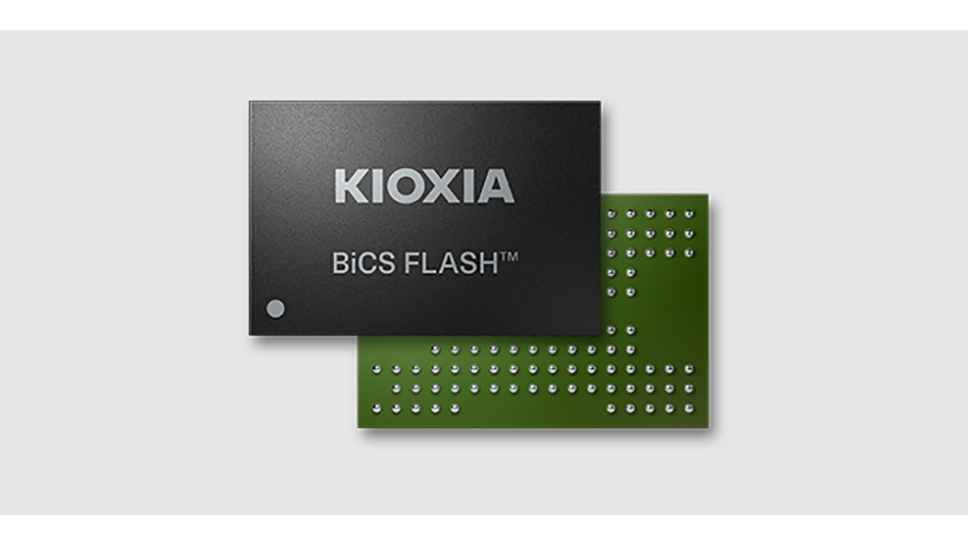
Kioxia Ships 10th Gen 332-Layer 3D Flash Samples
💡New high-density storage hardware is essential for scaling AI data centers and reducing infrastructure overhead.
⚡ 30-Second TL;DR
What Changed
10th generation BiCS FLASH technology with 332-layer stacking
Why It Matters
Increased NAND density is critical for training and inference workloads that require massive datasets. This advancement helps lower the cost-per-bit for AI infrastructure storage.
What To Do Next
Evaluate your data pipeline storage requirements; consider how higher-density SSDs could reduce your rack space and power consumption for large-scale model training.
Key Points
- •10th generation BiCS FLASH technology with 332-layer stacking
- •1Tb (Terabit) TLC memory device capacity
- •Optimized for enterprise-grade and AI data center SSDs
🧠 Deep Insight
AI-generated analysis for this event — not the original article.
🔑 Enhanced Key Takeaways
- •The 10th generation BiCS FLASH utilizes a new CBA (CMOS Directly Bonded to Array) architecture to enhance bit density and I/O performance.
- •Kioxia has achieved a significant increase in I/O speed, targeting over 3.2 Gbps to support the high-bandwidth requirements of AI training clusters.
- •The 332-layer process node incorporates advanced channel hole etching technology to maintain structural integrity and reliability at extreme aspect ratios.
- •This generation focuses on reducing power consumption per bit by approximately 15% compared to the 9th generation, addressing thermal constraints in high-density server racks.
- •Kioxia is leveraging its joint venture manufacturing facilities with Western Digital to accelerate the mass production ramp-up of this 332-layer node.
📊 Competitor Analysis▸ Show
| Feature | Kioxia 10th Gen (332L) | Samsung V-NAND (9th/10th Gen) | Micron G9 (232L+) |
|---|---|---|---|
| Layer Count | 332 | ~300+ (Gen 9/10) | 232+ (G9) |
| Architecture | CBA (CMOS Bonded) | COP (Cell on Peri) | CMOS Under Array |
| Target Market | AI Data Centers | Enterprise/Mobile | High-Performance SSDs |
| Status | Sampling | Mass Production | Mass Production |
🛠️ Technical Deep Dive
- Architecture: Utilizes CBA (CMOS Directly Bonded to Array) technology which separates the CMOS logic wafer from the memory cell array wafer before bonding to maximize wafer utilization.
- Cell Structure: Employs a multi-tier stacking process to achieve 332 layers while maintaining vertical channel hole uniformity.
- Interface: Supports high-speed NAND interface protocols (ONFI 5.x) to enable data transfer rates exceeding 3.2 Gbps.
- Capacity: 1Tb (128GB) per die using TLC (Triple-Level Cell) technology, optimized for high-density 3D NAND packages.
- Power Management: Integrated low-voltage operation modes designed specifically for AI-driven data center workloads that require constant high-throughput access.
🔮 Future ImplicationsAI analysis grounded in cited sources
⏳ Timeline
Weekly AI Recap
Read this week's curated digest of top AI events →
👉Related Updates


AI-curated news aggregator. All content rights belong to original publishers.
Original source: cnBeta (Full RSS) ↗
This is a summary, not the original. Read the source, or get the weekly briefing.
Weekly AI briefing
One email a week. Unsubscribe anytime.