Japan Tightens the AI Hardware Pipeline
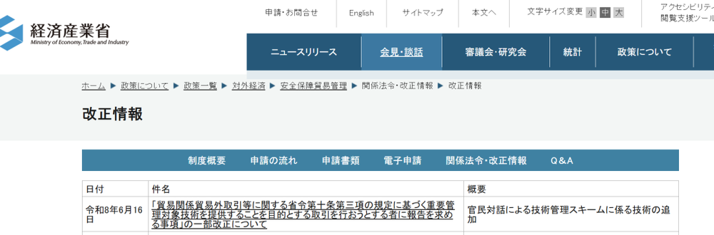
💡New controls target the materials and know-how behind AI servers, robots, power devices, and sensing hardware.
⚡ 30-Second TL;DR
What Changed
The new controls cover five strategic areas spanning electronics materials, compound semiconductors, magnets, next-generation photovoltaics, and radiation detection.
Why It Matters
AI infrastructure companies may face longer qualification cycles, alternative-material requirements, and increased supplier concentration risk. The policy also accelerates regionalization of semiconductor and advanced-material supply chains, especially for AI servers, robotics, power electronics, and imaging systems.
What To Do Next
Map your AI hardware bill of materials against the five newly controlled categories and qualify at least one non-Japanese supplier for each critical dependency.
Key Points
- •The new controls cover five strategic areas spanning electronics materials, compound semiconductors, magnets, next-generation photovoltaics, and radiation detection.
- •Companies may need to report technology transfers to Japan’s Ministry of Economy, Trade and Industry and wait 30 days or longer before proceeding.
- •Japan claims strong positions in GaN substrates and solder-resist materials, while seeking future advantages in perovskite photovoltaics and rare-earth-free magnets.
- •The controls regulate not only physical exports but also manufacturing know-how shared with overseas entities and research organizations.
🧠 Deep Insight
Background and context from public sources — not the original article. 11 sources cited.
🔑 Enhanced Key Takeaways
- •Japan's regulatory expansion is part of a broader 370 trillion yen investment roadmap aimed at securing 17 strategic sectors by 2040.
- •The government has specifically earmarked 68 trillion yen for the semiconductor sector and 10.5 trillion yen for 'physical AI' to bolster domestic hardware sovereignty.
- •The new reporting requirements complement existing export controls on high-end manufacturing tools like EUV lithography and atomic layer deposition systems.
- •Japan is actively leveraging its 2nm production initiative via Rapidus to create a domestic anchor for the global AI hardware supply chain.
- •The policy shift reflects a strategic pivot to regain global standard-setting influence in AI and semiconductor technologies, countering market dominance by the U.S., China, and South Korea.
🛠️ Technical Deep Dive
- GaN Substrates: Focus on high-frequency, high-power density applications for AI server power delivery systems.
- Solder Resist: Advanced materials optimized for high-density interconnect (HDI) substrates required by next-generation AI accelerators.
- Perovskite Batteries/Photovoltaics: Integration of thin-film materials to improve energy density and efficiency in edge-AI sensing devices.
- Scintillators: High-sensitivity radiation detection materials critical for precision manufacturing inspection and advanced medical imaging hardware.
- 2nm Node: Development of gate-all-around (GAA) transistor architectures to improve power efficiency and performance for AI training workloads.
🔮 Future ImplicationsAI analysis grounded in cited sources
⏳ Timeline
📎 Sources (11)
Factual claims are grounded in the sources below. Forward-looking analysis is AI-generated interpretation.
Weekly AI Recap
Read this week's curated digest of top AI events →
👉Related Updates


AI-curated news aggregator. All content rights belong to original publishers.
Original source: 虎嗅 ↗
This is a summary, not the original. Read the source, or get the weekly briefing.
Weekly AI briefing
One email a week. Unsubscribe anytime.