🌍The Next Web (TNW)•Stalecollected in 3h
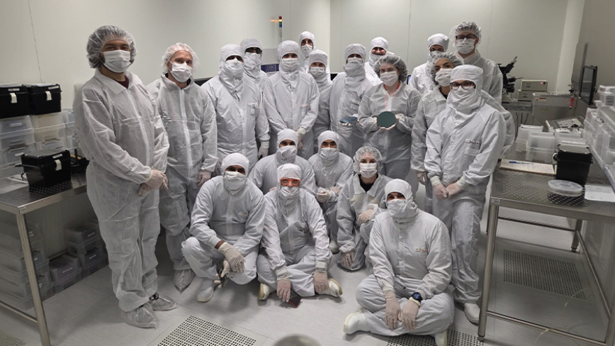
Italian Deeptech Bags €211M for Graphene Optical Chips
💡€211M scales graphene optics—key for faster AI interconnects
⚡ 30-Second TL;DR
What Changed
€211M Italian state aid approved by EU Commission
Why It Matters
Boosts photonic tech scaling for high-speed AI interconnects, potentially reducing latency in data centers. Positions Europe as contender in AI hardware innovation.
What To Do Next
Assess graphene photonics prototypes for AI cluster interconnect upgrades in your infrastructure plans.
Who should care:Researchers & Academics
🧠 Deep Insight
AI-generated analysis for this event.
🔑 Enhanced Key Takeaways
- •The funding is part of the IPCEI (Important Project of Common European Interest) on Microelectronics and Communication Technologies, aimed at reducing European dependency on non-EU semiconductor supply chains.
- •CamGraPhIC's technology utilizes graphene-based modulators which claim to offer significantly higher bandwidth density and lower power consumption compared to traditional silicon photonics.
- •The pilot line is specifically designed to bridge the 'valley of death' in deeptech, transitioning from laboratory-scale graphene wafer fabrication to high-volume CMOS-compatible manufacturing processes.
🛠️ Technical Deep Dive
- •Graphene-based electro-optic modulators: Leverages the high carrier mobility of graphene to achieve ultra-fast modulation speeds exceeding 100 GHz.
- •CMOS Integration: The manufacturing process is designed to be back-end-of-line (BEOL) compatible, allowing graphene layers to be integrated directly onto standard silicon-on-insulator (SOI) photonic circuits.
- •Energy Efficiency: Targets a reduction in energy-per-bit consumption by approximately 40-60% compared to current state-of-the-art silicon-based Mach-Zehnder modulators.
- •Thermal Stability: Graphene's high thermal conductivity assists in heat dissipation at the chip level, reducing the need for active cooling in high-density optical interconnects.
🔮 Future ImplicationsAI analysis grounded in cited sources
CamGraPhIC will achieve commercial-grade wafer yields by 2027.
The establishment of a dedicated pilot line is the critical prerequisite for stabilizing the manufacturing process required for high-volume commercial viability.
The project will trigger a shift in European data center architecture toward graphene-based interconnects.
State-backed industrialization projects of this scale are designed to create local supply chain ecosystems that favor the adoption of the subsidized technology over imported alternatives.
⏳ Timeline
2022-09
2D Photonics establishes CamGraPhIC as a dedicated subsidiary to focus on graphene photonic interconnects.
2024-06
CamGraPhIC completes initial prototype testing of graphene-on-silicon modulators at the wafer scale.
2026-03
European Commission grants formal state aid approval for the €211M industrialization project.
📰
Weekly AI Recap
Read this week's curated digest of top AI events →
👉Related Updates


AI-curated news aggregator. All content rights belong to original publishers.
Original source: The Next Web (TNW) ↗