Intel Alliance Advances Glass Substrate Packaging
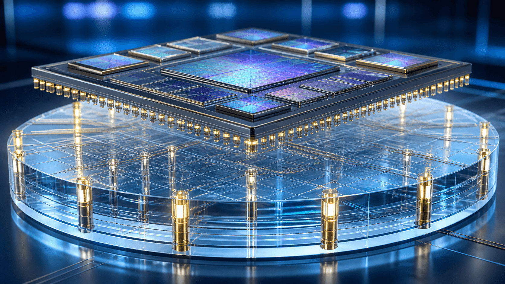
Glass packaging could reshape AI accelerator density, but TGV yield and cost remain the hurdles.
30-Second TL;DR
What Changed
Intel and Lens Technology are collaborating to accelerate glass substrate packaging.
Why It Matters
Glass substrates could improve packaging density and signal performance for advanced AI accelerators, but manufacturing reliability remains a constraint. A successful alliance may strengthen the supply chain for future high-bandwidth, high-density AI systems.
What To Do Next
Ask your AI hardware team to benchmark glass-substrate suppliers on TGV yield, RDL layer count, thermal performance, and projected cost per package.
Key Points
- •Intel and Lens Technology are collaborating to accelerate glass substrate packaging.
- •Triassic and Tongge Micro are working to overcome glass substrate brittleness.
- •Through-glass via yield is a major manufacturing bottleneck.
- •Multilayer RDL interconnects and scale economics will determine commercialization.
Deep Insight
AI-generated analysis for this event — not the original article.
Enhanced Key Takeaways
- •Glass substrates offer superior mechanical, physical, and optical properties compared to organic substrates, specifically enabling better flatness and thermal stability for large-scale chiplet integration.
- •The transition to glass substrates is driven by the need to support higher interconnect density and larger package sizes required by next-generation AI and high-performance computing (HPC) processors.
- •Lens Technology's involvement leverages their expertise in precision glass processing and surface treatment, which is critical for mitigating the inherent fragility of glass during the assembly process.
- •Intel's glass substrate roadmap is a key component of its '5 nodes in 4 years' strategy, aiming to maintain leadership in advanced packaging beyond the limitations of current silicon interposers.
- •The industry-wide shift toward glass is supported by the formation of the Glass Substrate Consortium, which aims to standardize manufacturing processes and material specifications to reduce ecosystem fragmentation.
Competitor Analysis
- Intel (Glass Substrate)
- High-performance AI/HPC
- Samsung Electro-Mechanics
- Mobile/Consumer Electronics
- SKC (Absolics)
- High-density Data Center
- Intel (Glass Substrate)
- Pilot/Pre-production
- Samsung Electro-Mechanics
- Pilot Production
- SKC (Absolics)
- Pilot Production
- Intel (Glass Substrate)
- Vertical integration
- Samsung Electro-Mechanics
- Existing substrate supply chain
- SKC (Absolics)
- Specialized glass material science
| Feature | Intel (Glass Substrate) | Samsung Electro-Mechanics | SKC (Absolics) |
|---|---|---|---|
| Primary Focus | High-performance AI/HPC | Mobile/Consumer Electronics | High-density Data Center |
| Maturity | Pilot/Pre-production | Pilot Production | Pilot Production |
| Key Advantage | Vertical integration | Existing substrate supply chain | Specialized glass material science |
Technical Deep Dive
- Through-Glass Via (TGV) technology utilizes laser drilling and chemical etching to create high-aspect-ratio holes for vertical electrical connections.
- Multilayer Redistribution Layers (RDL) are deposited on the glass surface to facilitate fine-pitch routing, significantly reducing signal loss compared to organic alternatives.
- Glass substrates exhibit a Coefficient of Thermal Expansion (CTE) that is more closely matched to silicon, reducing warpage during the thermal cycling of high-power chips.
- The manufacturing process involves specialized handling equipment to manage glass panels, which are prone to edge chipping and micro-cracking during traditional pick-and-place operations.
Future ImplicationsAI analysis grounded in cited sources
Timeline
- 2023-09Intel officially unveils its glass substrate development roadmap for next-generation packaging.
- 2024-05Intel announces the opening of a glass substrate research and development line in Arizona.
- 2025-02Intel and key ecosystem partners demonstrate initial TGV yield improvements for large-format panels.
- 2026-03Intel expands strategic partnerships with specialized glass manufacturers to secure supply chain readiness.
Weekly AI Recap
Read this week's curated digest of top AI events →
Related Updates




AI-curated news aggregator. All content rights belong to original publishers.
Original source: Pandaily ↗
This is a summary, not the original. Read the source, or get the weekly briefing.
The weekly digest
One email a week. Unsubscribe anytime.