HBF Could Add Terabytes to GPU Memory
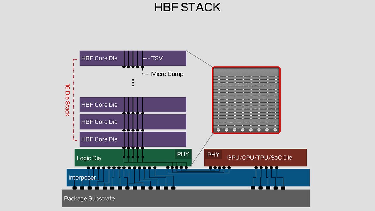
HBF targets terabytes of extra GPU memory, potentially changing large-model serving economics.
30-Second TL;DR
What Changed
HBF is designed to extend GPU memory capacity using NAND-based stacks.
Why It Matters
If ecosystem support develops, HBF could let AI systems handle larger models and datasets without relying solely on expensive HBM. Its practical impact remains uncertain because the specification is early-stage and broad industry adoption is not yet established.
What To Do Next
Track HBF specification revisions and prototype support before designing a GPU serving platform around NAND-backed memory expansion.
Key Points
- •HBF is designed to extend GPU memory capacity using NAND-based stacks.
- •The specification supports up to 16-Hi NAND stacks and targets up to 3 TB/s bandwidth.
- •UCIe is part of the proposed interconnect approach, but only four companies currently show interest.
Deep Insight
AI-generated analysis for this event — not the original article.
Enhanced Key Takeaways
- •HBF (High Bandwidth Flash) utilizes a tiered memory hierarchy that positions NAND as a capacity-extending layer behind traditional HBM3e/HBM4, effectively creating a 'near-memory' storage tier.
- •The architecture leverages the UCIe (Universal Chiplet Interconnect Express) standard to enable low-latency, die-to-die communication between the GPU compute die and the NAND controller.
- •Sandisk and SK hynix are positioning HBF as a solution to the 'memory wall' in Large Language Model (LLM) inference, allowing massive model weights to reside closer to the GPU than traditional NVMe SSDs.
- •The 16-Hi NAND stack configuration utilizes advanced hybrid bonding techniques to maintain signal integrity at the high-density levels required for terabyte-scale capacity.
- •Initial industry feedback suggests HBF aims to reduce the total cost of ownership (TCO) for AI servers by minimizing the reliance on expensive, high-capacity HBM stacks for static model parameters.
Competitor Analysis
- HBF (Sandisk/SK hynix)
- Near-memory (Low)
- CXL-based Memory Expansion
- Moderate (CXL overhead)
- Traditional NVMe SSDs
- High (PCIe/OS overhead)
- HBF (Sandisk/SK hynix)
- Up to 3 TB/s
- CXL-based Memory Expansion
- Limited by CXL 3.0/4.0
- Traditional NVMe SSDs
- Limited by PCIe Gen5/6
- HBF (Sandisk/SK hynix)
- GPU Model Weight Storage
- CXL-based Memory Expansion
- System RAM Expansion
- Traditional NVMe SSDs
- General Storage
- HBF (Sandisk/SK hynix)
- Premium (NAND-based)
- CXL-based Memory Expansion
- Moderate
- Traditional NVMe SSDs
- Low
| Feature | HBF (Sandisk/SK hynix) | CXL-based Memory Expansion | Traditional NVMe SSDs |
|---|---|---|---|
| Latency | Near-memory (Low) | Moderate (CXL overhead) | High (PCIe/OS overhead) |
| Bandwidth | Up to 3 TB/s | Limited by CXL 3.0/4.0 | Limited by PCIe Gen5/6 |
| Primary Use | GPU Model Weight Storage | System RAM Expansion | General Storage |
| Pricing | Premium (NAND-based) | Moderate | Low |
Technical Deep Dive
- Architecture: Utilizes a disaggregated memory approach where NAND is treated as a memory-mapped device rather than a block-storage device.
- Interconnect: Employs UCIe 1.1/2.0 for chiplet-level integration, allowing for direct memory access (DMA) patterns between the GPU and the HBF stack.
- Stack Density: 16-Hi NAND stacks utilize 3D TLC or QLC NAND, optimized for high-throughput read operations required by transformer-based AI models.
- Controller Logic: Integrates a specialized memory controller within the HBF stack to handle wear leveling and error correction (ECC) without interrupting GPU compute cycles.
Future ImplicationsAI analysis grounded in cited sources
Timeline
- 2025-06SK hynix and Sandisk announce strategic partnership for next-gen memory architectures.
- 2026-02Initial whitepaper on HBF (High Bandwidth Flash) concept presented at industry memory summit.
- 2026-08Formal introduction of the HBF specification and UCIe integration roadmap.
Weekly AI Recap
Read this week's curated digest of top AI events →
AI-curated news aggregator. All content rights belong to original publishers.
Original source: Tom's Hardware ↗
This is a summary, not the original. Read the source, or get the weekly briefing.
The weekly digest
One email a week. Unsubscribe anytime.