來源Tom's Hardware•較早收集於 16h
HBF 可為 GPU 增加數 TB 記憶體
#gpu-memory#nand#hbm-alternative#memory-bandwidthhbf-specificationsandisksk hynixhbfucie
HBF 瞄準數 TB 額外 GPU 記憶體,可能改變大型模型服務的成本結構。
30 秒速覽
有什麼變化
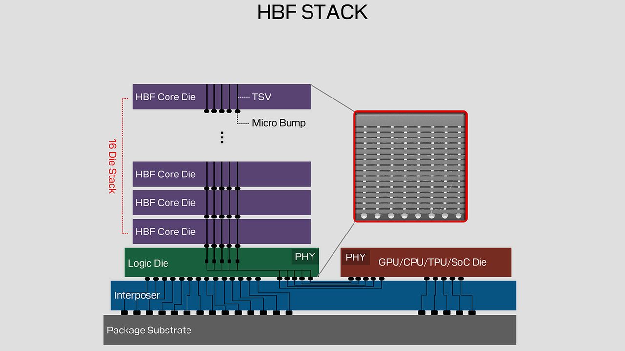
HBF 設計上透過 NAND 堆疊擴充 GPU 記憶體容量。
為什麼重要
若生態系統逐步成熟,HBF 可讓 AI 系統處理更大的模型與資料集,而不必完全依賴昂貴的 HBM。由於規格仍處於早期階段,且產業採用尚未普及,其實際影響仍不確定。
下一步行動
在以 NAND 支援的記憶體擴充方案設計 GPU 服務平台前,請先追蹤 HBF 規格修訂版本與原型支援情況。
誰應關注:Researchers & Academics
關鍵要點
- •HBF 設計上透過 NAND 堆疊擴充 GPU 記憶體容量。
- •該規格支援最高 16-Hi NAND 堆疊,並以最高 3 TB/s 頻寬為目標。
- •UCIe 是其連接方案的一部分,但目前僅有四家公司表達興趣。
深度解析
本篇為 AI 生成分析,非原文內容。
增強重點摘要
- •HBF (High Bandwidth Flash) utilizes a tiered memory hierarchy that positions NAND as a capacity-extending layer behind traditional HBM3e/HBM4, effectively creating a 'near-memory' storage tier.
- •The architecture leverages the UCIe (Universal Chiplet Interconnect Express) standard to enable low-latency, die-to-die communication between the GPU compute die and the NAND controller.
- •Sandisk and SK hynix are positioning HBF as a solution to the 'memory wall' in Large Language Model (LLM) inference, allowing massive model weights to reside closer to the GPU than traditional NVMe SSDs.
- •The 16-Hi NAND stack configuration utilizes advanced hybrid bonding techniques to maintain signal integrity at the high-density levels required for terabyte-scale capacity.
- •Initial industry feedback suggests HBF aims to reduce the total cost of ownership (TCO) for AI servers by minimizing the reliance on expensive, high-capacity HBM stacks for static model parameters.
競品分析
Latency
- HBF (Sandisk/SK hynix)
- Near-memory (Low)
- CXL-based Memory Expansion
- Moderate (CXL overhead)
- Traditional NVMe SSDs
- High (PCIe/OS overhead)
Bandwidth
- HBF (Sandisk/SK hynix)
- Up to 3 TB/s
- CXL-based Memory Expansion
- Limited by CXL 3.0/4.0
- Traditional NVMe SSDs
- Limited by PCIe Gen5/6
Primary Use
- HBF (Sandisk/SK hynix)
- GPU Model Weight Storage
- CXL-based Memory Expansion
- System RAM Expansion
- Traditional NVMe SSDs
- General Storage
Pricing
- HBF (Sandisk/SK hynix)
- Premium (NAND-based)
- CXL-based Memory Expansion
- Moderate
- Traditional NVMe SSDs
- Low
| Feature | HBF (Sandisk/SK hynix) | CXL-based Memory Expansion | Traditional NVMe SSDs |
|---|---|---|---|
| Latency | Near-memory (Low) | Moderate (CXL overhead) | High (PCIe/OS overhead) |
| Bandwidth | Up to 3 TB/s | Limited by CXL 3.0/4.0 | Limited by PCIe Gen5/6 |
| Primary Use | GPU Model Weight Storage | System RAM Expansion | General Storage |
| Pricing | Premium (NAND-based) | Moderate | Low |
技術深入
- Architecture: Utilizes a disaggregated memory approach where NAND is treated as a memory-mapped device rather than a block-storage device.
- Interconnect: Employs UCIe 1.1/2.0 for chiplet-level integration, allowing for direct memory access (DMA) patterns between the GPU and the HBF stack.
- Stack Density: 16-Hi NAND stacks utilize 3D TLC or QLC NAND, optimized for high-throughput read operations required by transformer-based AI models.
- Controller Logic: Integrates a specialized memory controller within the HBF stack to handle wear leveling and error correction (ECC) without interrupting GPU compute cycles.
前景展望基於引用來源的 AI 分析
HBF will replace traditional NVMe storage for primary AI model weight loading by 2028.
The massive bandwidth advantage of HBF over PCIe-based storage makes it the only viable solution for loading multi-terabyte models in sub-second timeframes.
GPU manufacturers will begin integrating HBF controllers directly into their silicon interposers.
To achieve the 3 TB/s target, the physical distance between the GPU die and the NAND stack must be minimized, necessitating interposer-level integration.
時間線
2025-06
SK hynix and Sandisk announce strategic partnership for next-gen memory architectures.
2026-02
Initial whitepaper on HBF (High Bandwidth Flash) concept presented at industry memory summit.
2026-08
Formal introduction of the HBF specification and UCIe integration roadmap.
- 2025-06SK hynix and Sandisk announce strategic partnership for next-gen memory architectures.
- 2026-02Initial whitepaper on HBF (High Bandwidth Flash) concept presented at industry memory summit.
- 2026-08Formal introduction of the HBF specification and UCIe integration roadmap.
AI 週報
閱讀本週精選 AI 大事摘要 →
AI 策展新聞聚合。所有內容版權歸原始發布者所有。
原始來源: Tom's Hardware ↗
每週電子報
每週一封,可隨時退訂。