d-Matrix Stacks AI Compute on DRAM

💡A radically different accelerator design targets 100 TB/s by bonding AI compute directly to DRAM.
⚡ 30-Second TL;DR
What Changed
Raptor is positioned as a 3D DRAM accelerator for generative inference.
Why It Matters
Direct compute-to-memory integration could reduce data-movement bottlenecks in high-throughput inference. If the performance claims translate into deployable products, the approach could pressure conventional accelerator and memory architectures.
What To Do Next
Use a roofline-style inference benchmark to measure whether your models are limited by memory bandwidth, then compare that profile with Raptor's claimed 100 TB/s target.
Key Points
- •Raptor is positioned as a 3D DRAM accelerator for generative inference.
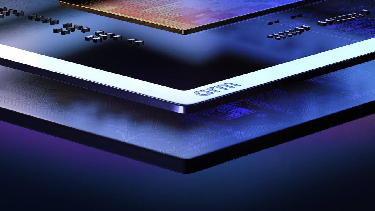
- •A TSMC 4nm compute die is bonded face-to-face onto a custom-designed DRAM die.
- •The design uses a 36-micron bonding pitch and targets 100 TB/s per card.
🧠 Deep Insight
Background and context from public sources — not the original article. 14 sources cited.
🔑 Enhanced Key Takeaways
- •The Raptor architecture utilizes an inverted logic design, placing the compute die on top of the DRAM to allow for direct contact with a cold plate for enhanced thermal management.
- •The DRAM die in the Raptor stack functions as an active interposer, routing PCIe and die-to-die signals through Through-Silicon Vias (TSVs) to minimize data travel distance.
- •d-Matrix is led by CEO Sid Sheth and CTO Sudeep Bhoja, who have a combined history of shipping over 100 million semiconductor units.
- •The company's strategic focus is on the AI inference market, which currently represents over 60% of total AI compute expenditure at major hyperscale data centers.
- •The Raptor architecture follows the successful launch of the Corsair platform, which reached full production status in June 2026.
📊 Competitor Analysis▸ Show
| Feature | d-Matrix (Raptor) | Cerebras | Groq | Etched |
|---|---|---|---|---|
| Primary Focus | 3D DRAM Inference | Wafer-Scale Training/Inference | LPU Inference | Transformer-Specific ASIC |
| Architecture | 3D Stacked DRAM | Wafer-Scale Engine | Tensor Streaming Processor | Fixed-Function Transformer |
| Market Position | TCO-focused Inference | High-throughput Training | Low-latency Inference | High-efficiency Inference |
🛠️ Technical Deep Dive
- 3D DRAM Stacking: Compute die bonded face-to-face with custom DRAM using a 36-micron bonding pitch.
- Thermal Management: Inverted logic layout places compute silicon on the top layer to facilitate direct liquid or air cooling via cold plate.
- Signal Routing: DRAM die acts as an interposer for PCIe and die-to-die interconnects using TSV technology.
- Process Node: Compute logic fabricated on TSMC 4nm process.
- Power Efficiency: Reduced power consumption achieved by minimizing physical distance between memory and compute logic.
🔮 Future ImplicationsAI analysis grounded in cited sources
⏳ Timeline
📎 Sources (14)
Factual claims are grounded in the sources below. Forward-looking analysis is AI-generated interpretation.
Weekly AI Recap
Read this week's curated digest of top AI events →
👉Related Updates


AI-curated news aggregator. All content rights belong to original publishers.
Original source: Tom's Hardware ↗
This is a summary, not the original. Read the source, or get the weekly briefing.
Weekly AI briefing
One email a week. Unsubscribe anytime.