CXMT DDR5 Yield Reaches 90%
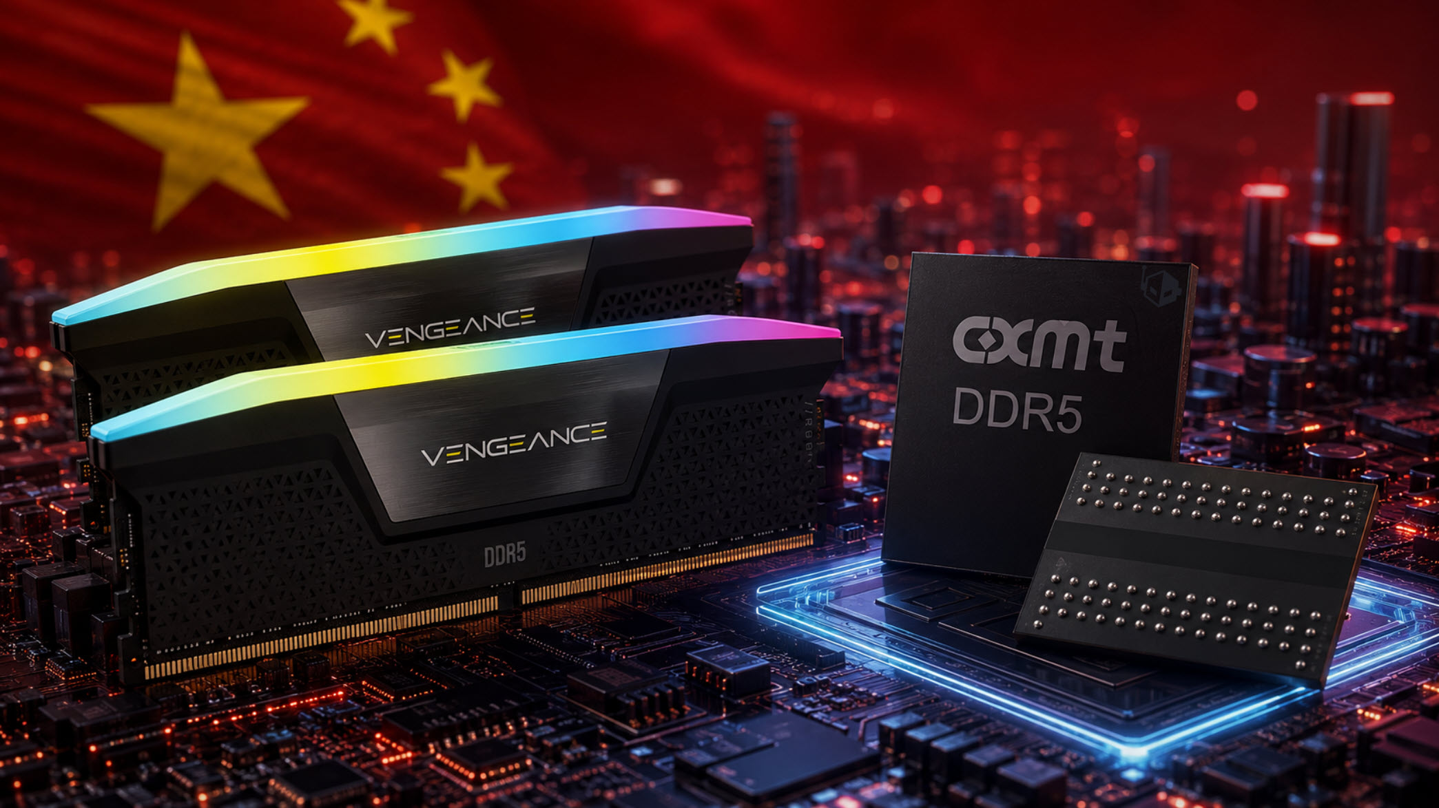
💡A reported 90% DDR5 yield could reshape memory sourcing for AI servers.
⚡ 30-Second TL;DR
What Changed
CXMT's DDR5 chips reportedly reached a 90% good-die yield.
Why It Matters
More competitive DDR5 supply could lower memory procurement risk for AI servers and other compute platforms. However, AI infrastructure buyers should still verify capacity, qualification status, performance, and long-term supply consistency before switching suppliers.
What To Do Next
Ask your AI server supplier to provide qualification data and sample availability for CXMT's 17nm DDR5 before planning a memory-source switch.
Key Points
- •CXMT's DDR5 chips reportedly reached a 90% good-die yield.
- •The chips use a 17nm-class manufacturing process.
- •Higher yield should support larger-scale production and shipments.
- •The progress may reduce CXMT's technology and supply gap with Micron.
🧠 Deep Insight
AI-generated analysis for this event.
🔑 Enhanced Key Takeaways
- •CXMT's 17nm-class process is widely considered a mature node that allows the company to bypass some of the most stringent EUV lithography restrictions currently imposed on Chinese semiconductor firms.
- •The 90% yield milestone is critical for CXMT's strategy to increase its market share in the domestic Chinese server and consumer PC markets, which are increasingly prioritizing 'secure and controllable' supply chains.
- •Industry analysts note that while CXMT has achieved parity in yield, they still face challenges in scaling to more advanced nodes like 10nm-class (1α or 1β) where competitors like Micron, Samsung, and SK Hynix currently dominate.
- •This yield improvement is expected to lower the per-unit cost of CXMT's DDR5 modules, potentially triggering a price war in the entry-level and mid-range memory segments within the Chinese market.
- •The company has been aggressively expanding its fab capacity in Hefei, with this yield milestone serving as a validation of their domestic equipment integration and process optimization efforts.
📊 Competitor Analysis▸ Show
| Feature | CXMT (17nm DDR5) | Micron (1α/1β nm DDR5) | Samsung (12nm-class DDR5) |
|---|---|---|---|
| Process Node | 17nm-class | 1α / 1β nm | 12nm-class |
| Market Position | Emerging / Domestic | Global Leader | Global Leader |
| EUV Usage | Minimal/None | High (for advanced nodes) | High (for advanced nodes) |
| Primary Focus | Cost-efficiency/Domestic | Performance/Enterprise | High-density/HBM/Mobile |
🛠️ Technical Deep Dive
- CXMT utilizes a proprietary DRAM architecture that leverages traditional DUV (Deep Ultraviolet) lithography combined with multi-patterning techniques to achieve 17nm feature sizes.
- The 17nm-class process relies on a capacitor-over-bitline (COB) cell structure, which is optimized for high-volume manufacturing stability rather than maximum density.
- DDR5 implementation includes on-die ECC (Error Correction Code) and dual-channel architecture, consistent with JEDEC standards, ensuring compatibility with mainstream Intel and AMD platforms.
- The process optimization focuses on reducing defect density in the peripheral circuitry, which has historically been a bottleneck for CXMT's yield ramp-up.
🔮 Future ImplicationsAI analysis grounded in cited sources
⏳ Timeline
Weekly AI Recap
Read this week's curated digest of top AI events →
👉Related Updates

AI-curated news aggregator. All content rights belong to original publishers.
Original source: cnBeta (Full RSS) ↗