Corning Glass Bridge enables optical interconnects for wafers
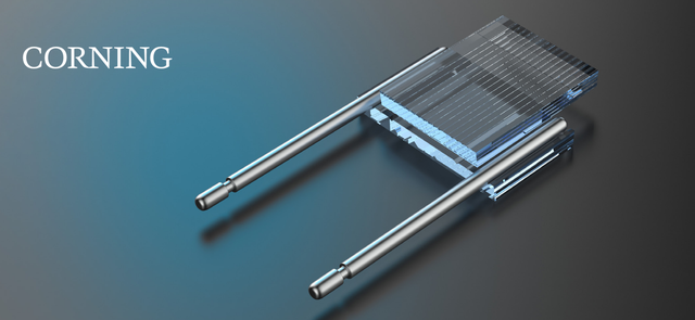
Lowering optical interconnect costs is critical for scaling next-gen AI data center performance.
30-Second TL;DR
What Changed
Reduces cost curves for optical interconnects
Why It Matters
This technology could lower the barrier for high-bandwidth AI hardware by improving chip-to-chip communication efficiency.
What To Do Next
Monitor Corning's technical whitepapers on glass-based optical interconnects for potential integration into future AI server architectures.
Key Points
- •Reduces cost curves for optical interconnects
- •Optimizes wafer-level manufacturing processes
- •Facilitates high-speed data communication infrastructure
Deep Insight
AI-generated analysis for this event — not the original article.
Enhanced Key Takeaways
- •Corning's Glass Bridge utilizes high-precision glass substrates to address the coefficient of thermal expansion (CTE) mismatch issues common in traditional silicon-based interposers.
- •The technology is specifically engineered to support Co-Packaged Optics (CPO) architectures, enabling closer integration between optical engines and high-performance compute (HPC) chips.
- •Glass Bridge leverages Corning's proprietary glass composition to provide superior signal integrity and lower dielectric loss compared to organic laminate substrates at frequencies exceeding 100 GHz.
- •The manufacturing process incorporates through-glass vias (TGV) with high aspect ratios, allowing for higher density interconnects than traditional through-silicon via (TSV) methods.
- •Corning is positioning this solution to mitigate the 'I/O bottleneck' in AI data centers by enabling massive parallel optical data transfer directly at the wafer level.
Competitor Analysis
- Corning Glass Bridge
- Ultra-Low
- Silicon Interposers (TSV)
- Moderate
- Organic Substrates
- High
- Corning Glass Bridge
- Excellent
- Silicon Interposers (TSV)
- Good
- Organic Substrates
- Poor
- Corning Glass Bridge
- Medium-High
- Silicon Interposers (TSV)
- High
- Organic Substrates
- Low
- Corning Glass Bridge
- High (Large Panel)
- Silicon Interposers (TSV)
- Limited (Wafer Size)
- Organic Substrates
- High
| Feature | Corning Glass Bridge | Silicon Interposers (TSV) | Organic Substrates |
|---|---|---|---|
| Signal Loss | Ultra-Low | Moderate | High |
| CTE Matching | Excellent | Good | Poor |
| Cost | Medium-High | High | Low |
| Scalability | High (Large Panel) | Limited (Wafer Size) | High |
Technical Deep Dive
- Substrate Material: Proprietary borosilicate or high-purity glass optimized for low dielectric constant (Dk) and dissipation factor (Df).
- Via Technology: Through-Glass Vias (TGV) with laser-drilling and metallization processes capable of sub-50 micron pitch.
- Thermal Stability: CTE matched to silicon to prevent warpage during high-temperature reflow processes.
- Interconnect Density: Supports multi-terabit per second (Tbps) bandwidth density required for next-generation AI accelerators.
- Integration: Compatible with standard flip-chip and surface-mount technology (SMT) assembly lines.
Future ImplicationsAI analysis grounded in cited sources
Timeline
- 2023-05Corning announces expansion of glass substrate manufacturing capabilities for semiconductor applications.
- 2024-11Corning showcases advanced TGV (Through-Glass Via) prototyping for high-performance computing.
- 2026-06Official launch of the 'Glass Bridge' platform for wafer-level optical interconnects.
Weekly AI Recap
Read this week's curated digest of top AI events →
AI-curated news aggregator. All content rights belong to original publishers.
Original source: 钛媒体 ↗
This is a summary, not the original. Read the source, or get the weekly briefing.
The weekly digest
One email a week. Unsubscribe anytime.