Chensi Tech secures funding for digital phased array chips
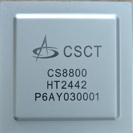
💡Learn how ASIC-based DBF chips are disrupting the phased array market by replacing FPGAs for better efficiency.
⚡ 30-Second TL;DR
What Changed
DBF chip replaces multiple FPGAs, reducing cost, power, and size
Why It Matters
The shift from FPGA-based solutions to ASIC-based DBF chips marks a significant step in the commercialization of high-performance phased array systems for mass-market applications.
What To Do Next
Monitor the performance metrics of ASIC-based DBF chips in low-altitude drone communication systems for potential integration in your hardware stack.
Key Points
- •DBF chip replaces multiple FPGAs, reducing cost, power, and size
- •Focuses on low-altitude economy, satellite internet, and radar applications
- •Achieved mass production in 2025 with full-stack design capabilities
🧠 Deep Insight
AI-generated analysis for this event — not the original article.
🔑 Enhanced Key Takeaways
- •Chensi Tech (Chengdu Chensi Technology Co., Ltd.) is headquartered in Chengdu, Sichuan, focusing on high-integration RF-SoC solutions.
- •The company's DBF chips utilize advanced CMOS process nodes to achieve high-density integration of analog-to-digital converters (ADC) and digital signal processing (DSP) units.
- •Their technology stack specifically targets the reduction of latency in phased array systems, which is critical for high-speed drone communication and satellite tracking.
- •The funding round is reportedly aimed at expanding R&D for next-generation millimeter-wave (mmWave) beamforming chips to support 6G research initiatives.
- •Chensi Tech has established strategic partnerships with domestic satellite constellation operators to integrate their chips into ground terminal equipment.
📊 Competitor Analysis▸ Show
| Feature | Chensi Tech (DBF SoC) | Traditional FPGA-based Solutions | Competitor (e.g., Analog Devices/TI) |
|---|---|---|---|
| Integration | High (SoC) | Low (Multi-chip) | Medium (Mixed-signal) |
| Power Consumption | Ultra-low | High | Moderate |
| Cost | Low (Mass production) | High | High |
| Size | Compact | Bulky | Moderate |
🛠️ Technical Deep Dive
- Architecture: Utilizes a highly integrated RF-SoC design that combines RF front-end, data conversion, and digital beamforming logic on a single die.
- Signal Processing: Implements on-chip digital beamforming algorithms that enable real-time phase and amplitude control for multi-beam steering.
- Process Node: Leverages advanced CMOS technology to optimize power-delay product, specifically targeting the 28nm or lower process nodes common in high-performance RF applications.
- Interface: Supports high-speed JESD204B/C or proprietary low-latency interfaces for seamless integration with baseband processors.
- Bandwidth: Designed to support wideband operation suitable for both Ka-band satellite links and low-altitude drone communication bands.
🔮 Future ImplicationsAI analysis grounded in cited sources
⏳ Timeline
Weekly AI Recap
Read this week's curated digest of top AI events →
👉Related Updates
AI-curated news aggregator. All content rights belong to original publishers.
Original source: 36氪 ↗
This is a summary, not the original. Read the source, or get the weekly briefing.
Weekly AI briefing
One email a week. Unsubscribe anytime.