Bengbu Builds a Full Domestic Sensor Stack
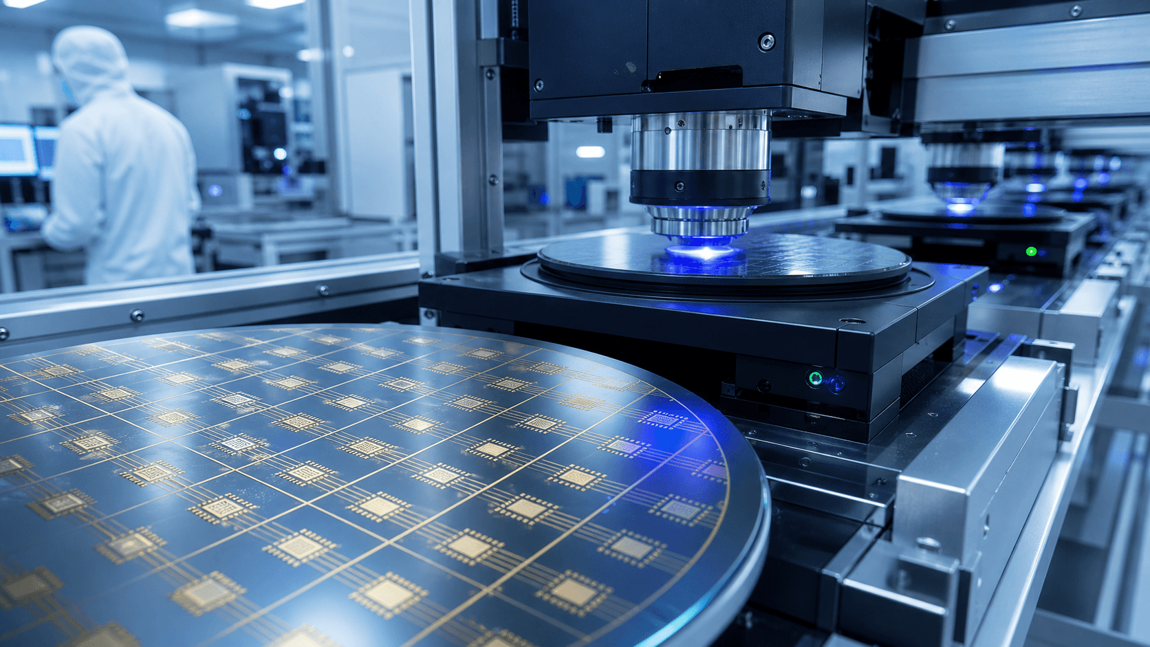
Bengbu’s end-to-end sensor stack could lower the barrier to building practical neuro-AI systems.
30-Second TL;DR
What Changed
Bengbu supports domestic 8-inch MEMS wafer production.
Why It Matters
A vertically integrated sensor supply chain could make neurotechnology prototypes easier to develop and deploy domestically. AI teams may gain more control over sensor data quality and hardware iteration, although clinical validation and data governance remain critical barriers.
What To Do Next
Use MNE-Python to build a reproducible EEG preprocessing pipeline and test it on stroke-rehabilitation or Alzheimer’s-related public datasets before integrating new BCI hardware.
Key Points
- •Bengbu supports domestic 8-inch MEMS wafer production.
- •The local ecosystem includes flexible brain-computer interface electrodes.
- •Clinical applications cover stroke rehabilitation and Alzheimer’s screening.
- •The city connects sensor manufacturing with biomedical deployment.
Deep Insight
AI-generated analysis for this event — not the original article.
Enhanced Key Takeaways
- •The Bengbu sensor initiative is anchored by the Bengbu MEMS Industrial Park, which serves as a specialized cluster for semiconductor and sensor manufacturing in Anhui province.
- •The 8-inch MEMS production line is specifically optimized for high-volume manufacturing of sensors used in IoT, automotive, and medical diagnostic devices.
- •Bengbu's BCI electrode development leverages flexible polyimide-based substrates to improve signal-to-noise ratios and biocompatibility for long-term neural monitoring.
- •The city has established a 'Sensor + AI' collaborative framework, integrating local sensor hardware with cloud-based diagnostic algorithms for Alzheimer's early detection.
- •Local government policy in Bengbu provides specific subsidies for 'domestic substitution' projects, aiming to reduce reliance on imported MEMS components for critical medical infrastructure.
Competitor Analysis
- Bengbu MEMS Ecosystem
- Medical/BCI/Domestic Substitution
- Global MEMS Foundries (e.g., TSMC/STMicro)
- Consumer/Automotive/General Purpose
- Domestic Competitors (e.g., Wuxi/Suzhou Clusters)
- Industrial/Automotive/General Purpose
- Bengbu MEMS Ecosystem
- 8-inch
- Global MEMS Foundries (e.g., TSMC/STMicro)
- 8-inch & 12-inch
- Domestic Competitors (e.g., Wuxi/Suzhou Clusters)
- 6-inch & 8-inch
- Bengbu MEMS Ecosystem
- Fully Domestic/Localized
- Global MEMS Foundries (e.g., TSMC/STMicro)
- Global/Diversified
- Domestic Competitors (e.g., Wuxi/Suzhou Clusters)
- Mixed Domestic/Imported
- Bengbu MEMS Ecosystem
- High (Direct Hospital Linkage)
- Global MEMS Foundries (e.g., TSMC/STMicro)
- Low (Component Supplier Only)
- Domestic Competitors (e.g., Wuxi/Suzhou Clusters)
- Moderate (Device Manufacturer Linkage)
| Feature | Bengbu MEMS Ecosystem | Global MEMS Foundries (e.g., TSMC/STMicro) | Domestic Competitors (e.g., Wuxi/Suzhou Clusters) |
|---|---|---|---|
| Focus | Medical/BCI/Domestic Substitution | Consumer/Automotive/General Purpose | Industrial/Automotive/General Purpose |
| Wafer Size | 8-inch | 8-inch & 12-inch | 6-inch & 8-inch |
| Supply Chain | Fully Domestic/Localized | Global/Diversified | Mixed Domestic/Imported |
| Clinical Integration | High (Direct Hospital Linkage) | Low (Component Supplier Only) | Moderate (Device Manufacturer Linkage) |
Technical Deep Dive
- MEMS Fabrication: Utilization of 8-inch wafer processing lines specifically configured for MEMS (Micro-Electro-Mechanical Systems) to achieve higher yield and lower cost per unit compared to 6-inch legacy lines.
- BCI Electrodes: Implementation of flexible, thin-film electrode arrays using biocompatible materials that conform to cortical surfaces, reducing tissue inflammation and signal degradation.
- Signal Processing: Integration of low-power ASIC (Application-Specific Integrated Circuit) chips directly with sensor modules to enable edge computing for real-time stroke rehabilitation feedback.
- Diagnostic Algorithms: Deployment of machine learning models trained on localized clinical datasets to identify biomarkers for Alzheimer's disease from sensor-derived physiological data.
Future ImplicationsAI analysis grounded in cited sources
Timeline
- 2022-05Bengbu officially designates the MEMS Industrial Park as a key strategic development zone.
- 2023-11Completion and pilot operation of the 8-inch MEMS wafer production line.
- 2024-09First successful clinical validation of flexible BCI electrodes in local stroke rehabilitation centers.
- 2025-06Launch of the integrated Alzheimer's screening platform utilizing domestic sensor data.
Weekly AI Recap
Read this week's curated digest of top AI events →
Related Updates



AI-curated news aggregator. All content rights belong to original publishers.
Original source: Pandaily ↗
This is a summary, not the original. Read the source, or get the weekly briefing.
The weekly digest
One email a week. Unsubscribe anytime.