Intel Adopts ASML Lithography for Panther Lake Chips
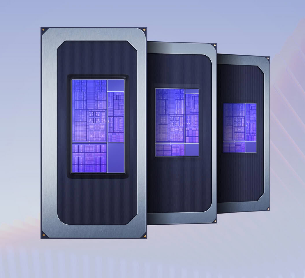
💡Critical infrastructure update for AI hardware: Intel's manufacturing shift impacts future edge AI chip availability.
⚡ 30-Second TL;DR
What Changed
Intel utilizes ASML's latest lithography machines for flagship chips
Why It Matters
This partnership strengthens Intel's ability to compete in the high-end mobile chip market by leveraging superior manufacturing precision. It signals a critical step in Intel's foundry strategy to regain process leadership.
What To Do Next
Monitor Intel's foundry roadmap updates to assess potential capacity shifts for AI-accelerated edge computing hardware.
Key Points
- •Intel utilizes ASML's latest lithography machines for flagship chips
- •Focus on manufacturing efficiency for Panther Lake architecture
- •Strategic move to master advanced semiconductor production equipment
🧠 Deep Insight
AI-generated analysis for this event.
🔑 Enhanced Key Takeaways
- •Panther Lake is manufactured on the Intel 18A process node, which leverages High-NA EUV lithography to achieve higher transistor density and improved power efficiency [1].
- •The integration of ASML's High-NA EUV (EXE:5000/5200) systems marks a critical shift in Intel's foundry strategy to regain process leadership against TSMC [1].
- •Panther Lake utilizes Intel's Foveros 3D packaging technology, allowing the integration of disparate chiplets (tiles) manufactured on different process nodes [1].
- •The adoption of these lithography tools is part of Intel's '5 nodes in 4 years' roadmap, specifically targeting the transition from RibbonFET gate-all-around transistors [1].
- •Intel's use of High-NA EUV is intended to reduce the number of multi-patterning steps required in traditional EUV, thereby lowering defect rates and production cycle times [1].
📊 Competitor Analysis▸ Show
| Feature | Intel Panther Lake (18A) | TSMC N2 (2nm) | Samsung 2nm (SF2) |
|---|---|---|---|
| Transistor Architecture | RibbonFET (GAA) | NanoFlex (GAA) | MBCFET (GAA) |
| Lithography | High-NA EUV | EUV (Low-NA) / Multi-patterning | EUV (Low-NA) |
| Primary Focus | Mobile/High-Performance | High-Performance/AI | Mobile/Foundry |
| Status (as of 2026) | In Production | In Production | In Production |
🛠️ Technical Deep Dive
- Process Node: Intel 18A (1.8nm class).
- Transistor Type: RibbonFET (Gate-All-Around).
- Power Delivery: PowerVia (Backside power delivery network).
- Lithography Equipment: ASML High-NA EUV (EXE:5000 series).
- Packaging: Foveros 3D chiplet architecture.
- Compute Tile: Likely utilizes Cougar Cove P-cores and Skymont E-cores.
🔮 Future ImplicationsAI analysis grounded in cited sources
⏳ Timeline
Weekly AI Recap
Read this week's curated digest of top AI events →
👉Related Updates




AI-curated news aggregator. All content rights belong to original publishers.
Original source: cnBeta (Full RSS) ↗