AI Optical Interconnects Set for 10x Market Growth
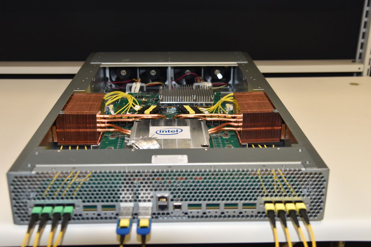
💡AI clusters may soon depend on a $144 billion optical interconnect market dominated by Silicon photonics.
⚡ 30-Second TL;DR
What Changed
The market is forecast to expand from $13.7 billion in 2024 to $144.4 billion by 2030.
Why It Matters
Rapid growth in optical interconnects could reshape the networking architectures used for large-scale AI training and inference. AI infrastructure teams may need to evaluate optical bandwidth, power efficiency, and integration strategies earlier in their cluster planning.
What To Do Next
Benchmark optical-network bandwidth and power requirements for your next AI cluster, including whether co-packaged optics could reduce interconnect bottlenecks.
Key Points
- •The market is forecast to expand from $13.7 billion in 2024 to $144.4 billion by 2030.
- •Silicon photonics is projected to account for 63.7% of total market revenue.
- •Co-packaged optics is identified as a major driver of future data center adoption.
- •The forecast implies more than ten-fold growth within six years.
🧠 Deep Insight
AI-generated analysis for this event.
🔑 Enhanced Key Takeaways
- •The surge in optical interconnect demand is primarily driven by the transition from pluggable transceivers to co-packaged optics (CPO) to overcome the 'bandwidth wall' in AI clusters.
- •Major hyperscalers like NVIDIA, Meta, and Microsoft are actively integrating silicon photonics to reduce power consumption per bit, which is critical for scaling GPU clusters beyond 100,000 units.
- •The shift toward optical I/O is enabling disaggregated data center architectures, allowing memory and compute resources to be physically separated while maintaining low-latency communication.
- •Thermal management remains a significant technical hurdle for CPO, as placing lasers and optical engines in close proximity to high-heat-generating ASICs requires advanced packaging solutions.
- •Foundry capacity for silicon photonics is expanding rapidly, with major players like TSMC, GlobalFoundries, and Intel investing in specialized manufacturing processes to support high-volume production.
📊 Competitor Analysis▸ Show
| Technology Approach | Key Players | Primary Advantage | Primary Challenge |
|---|---|---|---|
| Pluggable Optics | Coherent, Lumentum, InnoLight | Mature ecosystem, field-replaceable | Power/density limits at 800G+ |
| Co-Packaged Optics (CPO) | NVIDIA, Broadcom, Intel | Lowest power/latency, high density | Complex thermal/repairability |
| Optical I/O Chiplets | Ayar Labs, Lightmatter | Disaggregation, extreme bandwidth | Integration with existing CMOS |
| Silicon Photonics | GlobalFoundries, TSMC | Scalable manufacturing | Laser integration/reliability |
🛠️ Technical Deep Dive
- Silicon photonics utilizes standard CMOS fabrication processes to integrate optical components like modulators, waveguides, and photodetectors on silicon wafers.
- Co-packaged optics (CPO) moves the optical engine from the front panel to the substrate, significantly reducing the electrical trace length between the switch/GPU and the optical module.
- Optical I/O chiplets leverage wavelength division multiplexing (WDM) to increase data throughput over a single fiber by transmitting multiple data streams on different wavelengths.
- Advanced packaging techniques such as 2.5D and 3D stacking are essential for connecting the optical engine to the compute die with minimal signal loss.
- The transition to 1.6T and 3.2T pluggable and CPO modules is driving the adoption of higher-order modulation formats like PAM4 and potentially coherent optics for shorter reaches.
🔮 Future ImplicationsAI analysis grounded in cited sources
⏳ Timeline
Weekly AI Recap
Read this week's curated digest of top AI events →
👉Related Updates
AI-curated news aggregator. All content rights belong to original publishers.
Original source: Tom's Hardware ↗