🐼Pandaily•Freshcollected in 2h
AI Glasses Face the Impossible Triangle in Chip Design
💡Understand the hardware bottlenecks limiting the next generation of AI wearable devices.
⚡ 30-Second TL;DR
What Changed
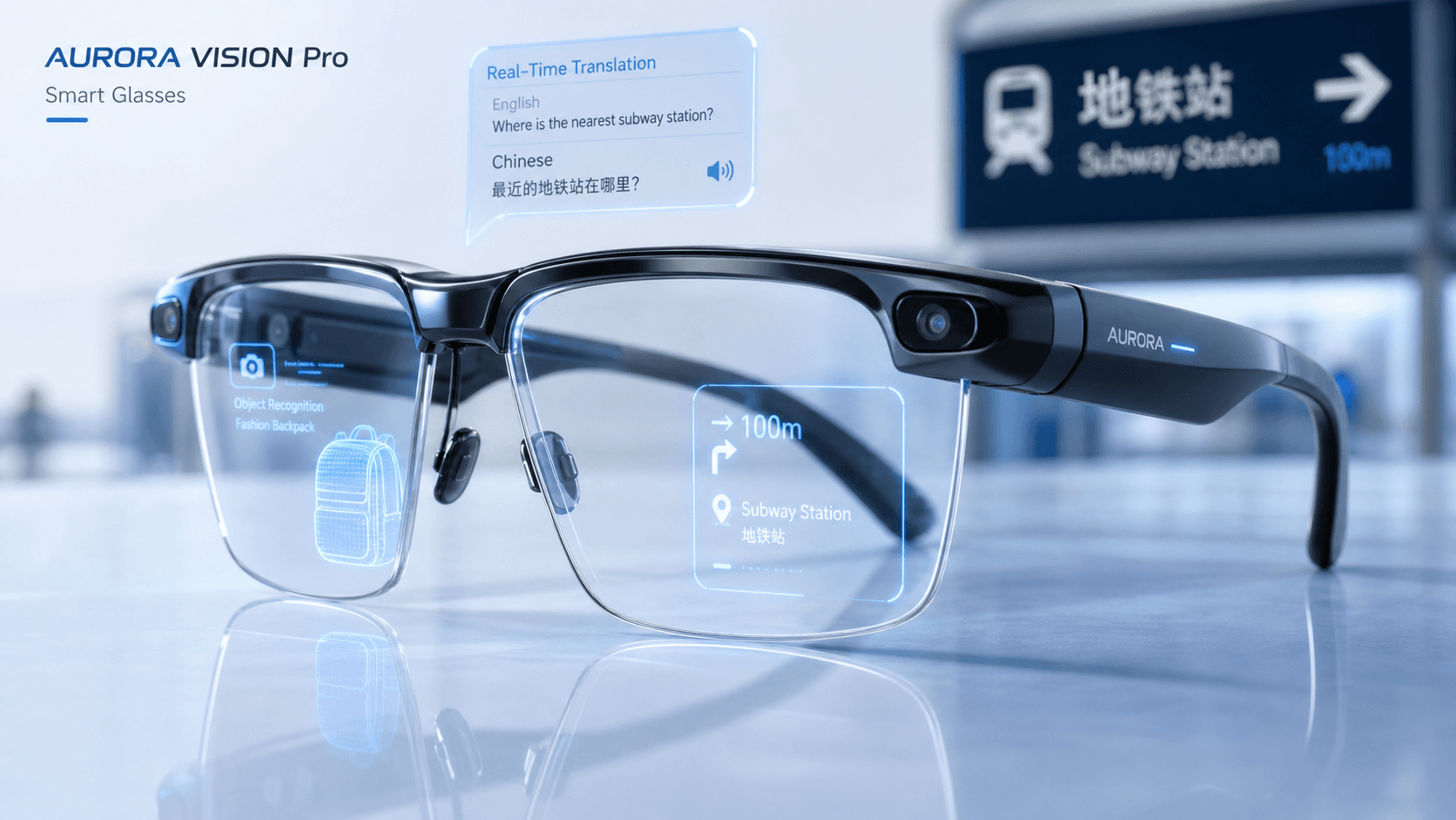
AI glasses face an 'impossible triangle' of cost, performance, and battery life.
Why It Matters
This highlights the hardware-level constraints for wearable AI, suggesting that future AI applications must be optimized for edge-compute efficiency rather than cloud-heavy processing.
What To Do Next
Evaluate edge-optimized model quantization techniques like INT8 or 4-bit to reduce the compute load for wearable AI deployments.
Who should care:Developers & AI Engineers
🧠 Deep Insight
AI-generated analysis for this event.
🔑 Enhanced Key Takeaways
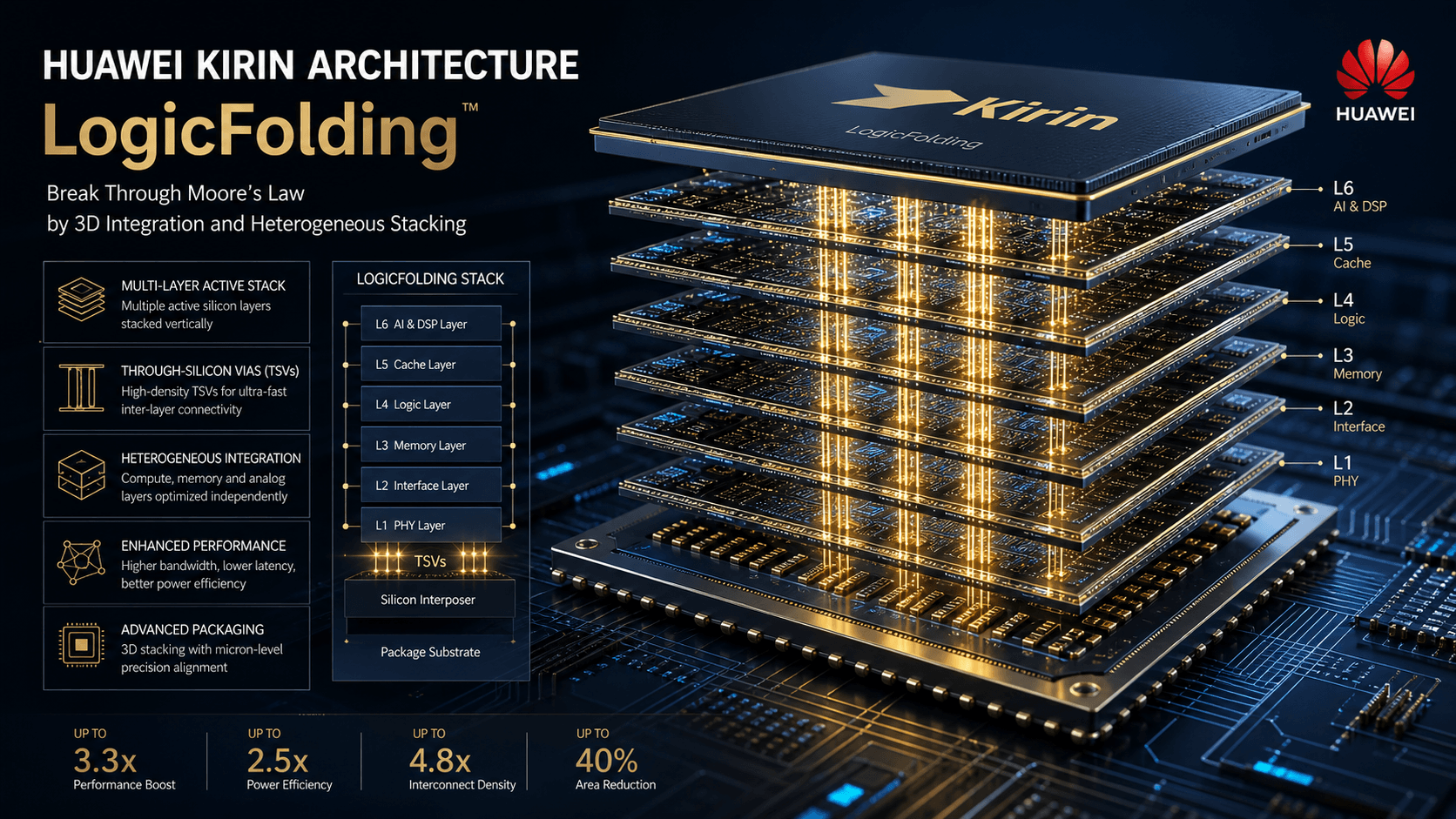
- •The 'impossible triangle' is exacerbated by the shift from cloud-based AI processing to on-device edge computing, which requires specialized NPU (Neural Processing Unit) integration within the SoC.
- •Advanced packaging technologies like FOWLP (Fan-Out Wafer-Level Packaging) are being adopted to reduce the physical footprint of the SoC, addressing the strict weight constraints of wearable glasses.
- •Industry standards are shifting toward heterogeneous computing architectures, where low-power microcontrollers handle 'always-on' sensor data while the primary AI accelerator remains in a deep-sleep state to conserve battery.
- •Thermal throttling in AI glasses is being mitigated by new material science applications, such as graphene-based heat spreaders integrated directly into the frame chassis.
- •Latency requirements for augmented reality (AR) overlays necessitate a motion-to-photon latency of under 20ms, forcing chip designers to prioritize deterministic AI inference over raw throughput.
📊 Competitor Analysis▸ Show
| Feature | Meta Orion (Prototype) | Snap Spectacles (Gen 5) | Ray-Ban Meta (Gen 2) |
|---|---|---|---|
| AI Processing | On-device + Cloud | On-device (Snap OS) | Cloud-heavy |
| Display | MicroLED AR | Waveguide AR | None (Audio/Camera) |
| Battery Life | ~2 Hours | ~45 Minutes | ~4 Hours |
| Primary Focus | AR Research | Developer/Creator | Lifestyle/Audio |
🛠️ Technical Deep Dive
- SoC Architecture: Transitioning to 3nm and 4nm process nodes to maximize performance-per-watt ratios for AI inference.
- Memory Bandwidth: Utilization of LPDDR5X or LPDDR5T memory to handle high-speed data transfer between the NPU and image signal processor (ISP).
- Thermal Design Power (TDP): Target envelopes for AI glasses are typically restricted to under 2-3W to prevent skin-contact discomfort.
- Sensor Fusion: Implementation of dedicated low-latency pipelines for IMU (Inertial Measurement Unit) and camera data to ensure stable AR tracking without overloading the main CPU.
🔮 Future ImplicationsAI analysis grounded in cited sources
Hardware-level AI acceleration will become the primary differentiator for consumer AR glasses by 2027.
As software complexity increases, general-purpose processors will fail to meet the latency requirements for real-time spatial computing.
Battery density improvements will plateau, forcing a shift toward external 'compute pucks' or wireless power transmission.
The physical constraints of glasses frames limit battery capacity, making current energy density insufficient for sustained high-performance AI tasks.
⏳ Timeline
2021-09
Meta and EssilorLuxottica launch first-generation Ray-Ban Meta smart glasses.
2023-10
Meta releases second-generation Ray-Ban Meta glasses with improved AI integration.
2024-09
Meta unveils Orion AR glasses prototype, showcasing advanced waveguide and silicon integration.
2024-09
Snap Inc. announces fifth-generation Spectacles with integrated AR display and custom OS.
📰
Weekly AI Recap
Read this week's curated digest of top AI events →
👉Related Updates

AI-curated news aggregator. All content rights belong to original publishers.
Original source: Pandaily ↗