Advanced Packaging Becomes AI’s New Scaling Engine
AI scaling is shifting from transistor counts to packaging bandwidth, bonding density, and HBM integration.
30-Second TL;DR
What Changed
The global advanced packaging market is estimated at $55 billion in 2025 and could exceed $120 billion by 2031.
Why It Matters
For AI infrastructure builders, packaging is becoming as strategically important as process nodes. Limited CoWoS and advanced bonding capacity may constrain accelerator shipments, system design choices, and total compute cost through 2027–2028.
What To Do Next
When planning your next AI accelerator or inference server, benchmark UCIe-based Chiplet designs and compare their bandwidth, latency, thermal, and packaging constraints with monolithic alternatives.
Key Points
- •The global advanced packaging market is estimated at $55 billion in 2025 and could exceed $120 billion by 2031.
- •UCIe 3.0 raises chiplet interconnect speeds to 48 GT/s and 64 GT/s, up from 32 GT/s in UCIe 2.0.
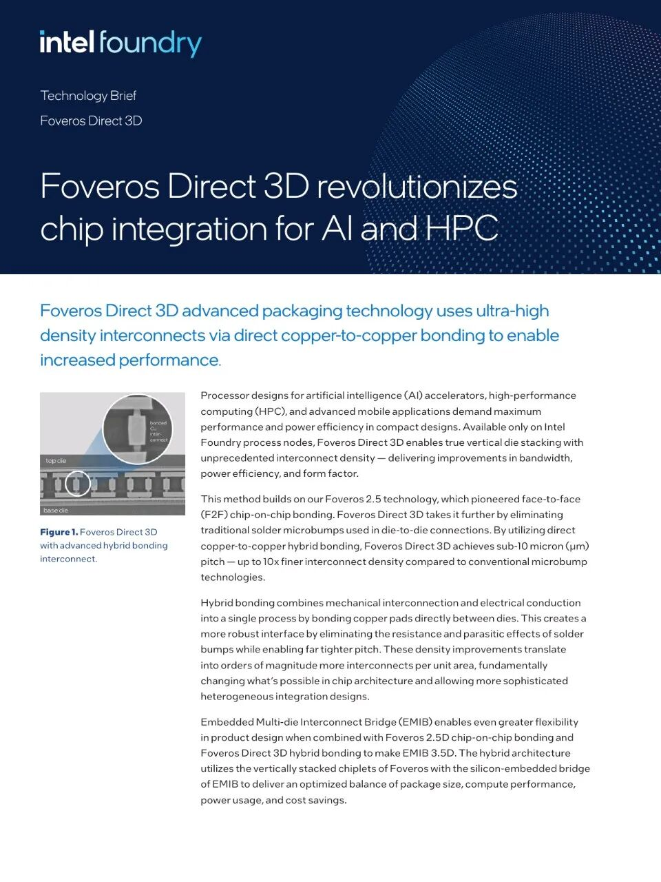
- •Intel’s Foveros Direct 3D uses sub-10μm copper-to-copper hybrid bonding and can increase interconnect density by approximately 10x.
- •TSMC’s CoWoS integrates AI processors with HBM and remains a major packaging bottleneck, despite planned capacity expansion.
Deep Insight
AI-generated analysis for this event — not the original article.
Enhanced Key Takeaways
- •The transition to glass substrates is emerging as a critical successor to organic interposers, offering superior thermal stability and finer routing density for next-generation AI accelerators.
- •Thermal management in 3D-stacked packages has become a primary failure point, leading to the adoption of microfluidic cooling and advanced thermal interface materials (TIMs) with higher conductivity.
- •Heterogeneous integration is driving a shift toward 'Chiplet-as-a-Service' models, where foundries provide standardized die-to-die interface IP and packaging design kits to fabless companies.
- •Power delivery networks (PDN) are being moved to the backside of the wafer (Backside Power Delivery) in advanced packaging to reduce IR drop and signal interference in high-current AI chips.
- •The standardization of Universal Chiplet Interconnect Express (UCIe) is being challenged by proprietary 'closed-loop' ecosystems that prioritize extreme low-latency performance over cross-vendor interoperability.
Competitor Analysis
- TSMC (CoWoS)
- High-volume AI/HPC
- Intel (Foveros)
- Heterogeneous 3D logic
- Samsung (I-Cube/X-Cube)
- Memory-logic integration
- TSMC (CoWoS)
- Micro-bump / Hybrid
- Intel (Foveros)
- Foveros Direct (Hybrid)
- Samsung (I-Cube/X-Cube)
- Hybrid / TSV
- TSMC (CoWoS)
- Industry Standard
- Intel (Foveros)
- High-end Custom
- Samsung (I-Cube/X-Cube)
- Cost-competitive/Foundry
| Feature | TSMC (CoWoS) | Intel (Foveros) | Samsung (I-Cube/X-Cube) |
|---|---|---|---|
| Primary Focus | High-volume AI/HPC | Heterogeneous 3D logic | Memory-logic integration |
| Bonding Tech | Micro-bump / Hybrid | Foveros Direct (Hybrid) | Hybrid / TSV |
| Market Position | Industry Standard | High-end Custom | Cost-competitive/Foundry |
Technical Deep Dive
- Hybrid Bonding: Eliminates solder bumps by using direct copper-to-copper connections, reducing interconnect pitch to <10μm and lowering parasitic capacitance.
- TSV (Through-Silicon Via) Scaling: Current high-density TSV processes are reaching aspect ratios of 10:1, enabling vertical stacking of 12-high and 16-high HBM3e/HBM4 stacks.
- Die-to-Die (D2D) Latency: UCIe 3.0 targets <10ns latency for chiplet-to-chiplet communication, essential for maintaining cache coherency in disaggregated AI processors.
- Substrate Materials: Shift from ABF (Ajinomoto Build-up Film) to glass-core substrates to mitigate warpage issues in large-area packages exceeding 1000mm².
Future ImplicationsAI analysis grounded in cited sources
Timeline
- 2011-06TSMC introduces CoWoS (Chip on Wafer on Substrate) technology.
- 2019-12Intel announces Foveros 3D packaging technology for heterogeneous chip stacking.
- 2022-03UCIe 1.0 specification is released, establishing an open standard for chiplet interconnects.
- 2024-08UCIe 2.0 specification is finalized, introducing support for advanced packaging and improved power efficiency.
- 2025-05TSMC announces major capacity expansion for CoWoS-L and CoWoS-R to address AI supply shortages.
Weekly AI Recap
Read this week's curated digest of top AI events →
AI-curated news aggregator. All content rights belong to original publishers.
Original source: 虎嗅 ↗
This is a summary, not the original. Read the source, or get the weekly briefing.
The weekly digest
One email a week. Unsubscribe anytime.