來源虎嗅•較早收集於 24m
高盛為何押注 HBM 價格近乎翻倍?
#memory#ai-chips#data-centers#supply-chainhbmgoldman-sachssk-hynixsamsung-electronicshbm4visible-alpha
HBM 價格可能近乎翻倍並重塑 AI 硬體成本,但關鍵假設仍待驗證。
30 秒速覽
有什麼變化
高盛預測 2027 年 HBM 混合平均售價約為每 Gb 2.9 美元,高於 Visible Alpha 約 2.3 美元的一致預期。
為什麼重要
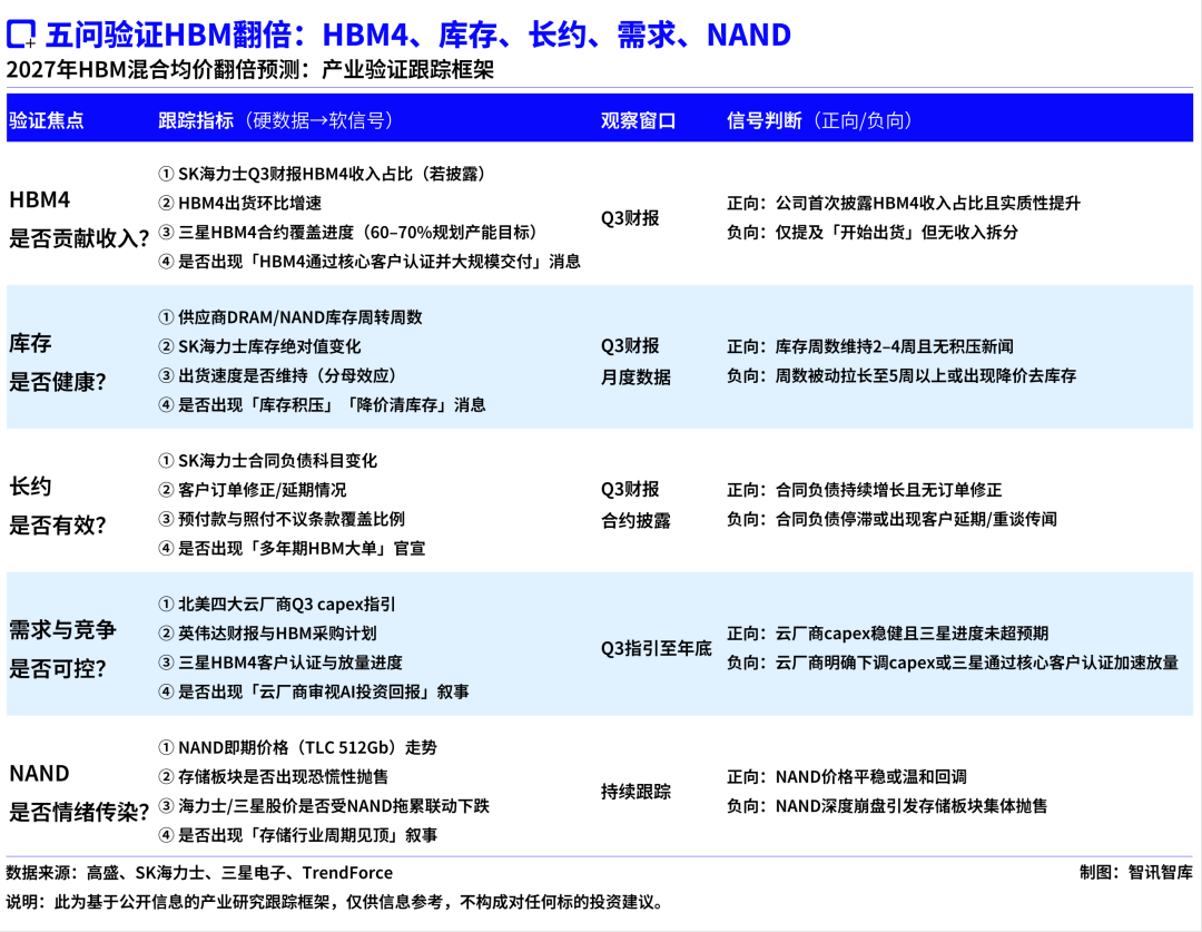
HBM 定價將直接影響 AI 加速器與資料中心專案的成本結構及產能規劃。AI 基礎設施採購方不應將高盛預測視為已確立的趨勢,因為 HBM4 良率、供應商競爭、合約條款與 AI 資本支出仍需透過季度數據驗證。
下一步行動
在 GPU 成本模型中加入 HBM4 良率、供應商配額與合約平均售價情境,並在 Samsung 或 SK hynix 公布第三季業績後更新假設。
誰應關注:Enterprise & Security Teams
關鍵要點
- •高盛預測 2027 年 HBM 混合平均售價約為每 Gb 2.9 美元,高於 Visible Alpha 約 2.3 美元的一致預期。
- •預期漲價建立在 HBM 供需缺口從 2026 年的 5.4% 擴大至 2027 年 6.0% 的基礎上。
- •通用 DRAM 價格可能在 2026 年底升至每 Gb 約 2.0 美元,為 HBM 合約重新定價提供錨點。
- •預測增幅約 40% 依賴產品組合改善與 HBM4 放量,但這部分的執行仍存在不確定性。
- •主要下行風險未必是 AI 需求崩潰,而是供給加速、競爭加劇與資本支出縮減同時發生。
深度解析
本篇為 AI 生成分析,非原文內容。
增強重點摘要
- •Goldman Sachs' bullish outlook is partially predicated on the transition to HBM4, which utilizes a 2048-bit interface compared to HBM3E's 1024-bit, significantly increasing manufacturing complexity and cost.
- •The supply-demand imbalance is exacerbated by the 'die size penalty' associated with advanced HBM nodes, where larger die sizes reduce the number of chips per wafer, effectively tightening supply even if wafer starts remain constant.
- •SK hynix has reportedly secured a dominant share of the HBM3E market for NVIDIA's Blackwell platform, creating a high barrier to entry for competitors attempting to capture margin through volume.
- •Samsung Electronics is aggressively pursuing the 'Custom HBM' strategy, aiming to integrate logic dies directly into the HBM stack to differentiate from standard commodity HBM offerings.
- •Market analysts note that the 'blended ASP' calculation is highly sensitive to the yield rates of 12-high and 16-high stacks, which currently face significant thermal and stacking challenges in mass production.
競品分析
Market Position
- SK Hynix (HBM3E/4)
- Current Leader
- Samsung (HBM3E/4)
- Aggressive Challenger
- Micron (HBM3E)
- Niche/Fast Follower
Key Advantage
- SK Hynix (HBM3E/4)
- High Yield/NVIDIA Partnership
- Samsung (HBM3E/4)
- Logic Integration/Foundry Synergy
- Micron (HBM3E)
- Power Efficiency
HBM4 Status
- SK Hynix (HBM3E/4)
- Development Phase
- Samsung (HBM3E/4)
- Development Phase
- Micron (HBM3E)
- Sampling Phase
| Feature | SK Hynix (HBM3E/4) | Samsung (HBM3E/4) | Micron (HBM3E) |
|---|---|---|---|
| Market Position | Current Leader | Aggressive Challenger | Niche/Fast Follower |
| Key Advantage | High Yield/NVIDIA Partnership | Logic Integration/Foundry Synergy | Power Efficiency |
| HBM4 Status | Development Phase | Development Phase | Sampling Phase |
技術深入
- HBM4 architecture shifts to a 2048-bit wide interface, doubling the bandwidth per stack compared to HBM3E.
- Implementation of 16-high stacking requires advanced MR-MUF (Mass Reflow Molded Underfill) or hybrid bonding techniques to manage thermal dissipation and vertical interconnect density.
- Logic die integration in HBM4 allows for custom base dies, enabling memory-side processing capabilities that reduce latency for AI inference workloads.
- Thermal management in 2026-era HBM relies on improved thermal conductivity materials (TC-NCF) to prevent localized hotspots during high-bandwidth operations.
前景展望基於引用來源的 AI 分析
HBM4 adoption will cause a structural shift in memory pricing models.
The transition to custom logic-integrated base dies moves HBM from a commodity component to an ASIC-like product, decoupling its price from standard DRAM cycles.
Samsung's foundry-memory synergy will become a critical differentiator by 2027.
The ability to manufacture the base logic die in-house provides a cost and integration advantage over competitors who must outsource base die fabrication.
時間線
2023-10
SK hynix announces mass production of HBM3E, setting the industry standard for high-capacity AI memory.
2024-02
Samsung Electronics unveils its 36GB HBM3E 12-high stack, focusing on high-density capacity for large language models.
2025-05
Industry-wide shift toward HBM4 development begins as AI accelerator requirements exceed HBM3E bandwidth limits.
2026-03
Samsung and SK hynix report record-high capital expenditure allocations specifically for HBM-dedicated TSV (Through-Silicon Via) capacity.
- 2023-10SK hynix announces mass production of HBM3E, setting the industry standard for high-capacity AI memory.
- 2024-02Samsung Electronics unveils its 36GB HBM3E 12-high stack, focusing on high-density capacity for large language models.
- 2025-05Industry-wide shift toward HBM4 development begins as AI accelerator requirements exceed HBM3E bandwidth limits.
- 2026-03Samsung and SK hynix report record-high capital expenditure allocations specifically for HBM-dedicated TSV (Through-Silicon Via) capacity.
AI 週報
閱讀本週精選 AI 大事摘要 →
AI 策展新聞聚合。所有內容版權歸原始發布者所有。
原始來源: 虎嗅 ↗
每週電子報
每週一封,可隨時退訂。