來源cnBeta (Full RSS)•較早收集於 3m
三星加速龍仁晶圓廠建設,投產時間提前至2029年
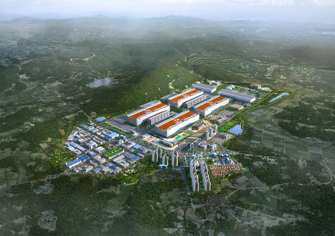
💡晶片投產時程提前,將直接影響下一代AI硬體的供應與成本。
⚡ 30 秒速覽
有什麼變化
三星首座龍仁晶圓廠預計於2029年投產
為什麼重要
投產時間提前將提升全球高階晶片的供應能力,長期來看有助於降低AI硬體開發者的成本。
下一步行動
密切關注三星的晶圓代工路線圖更新,以便為未來的AI基礎設施專案調整硬體採購策略。
誰應關注:Enterprise & Security Teams
關鍵要點
- •三星首座龍仁晶圓廠預計於2029年投產
- •受惠於政府支持,投產時間較原計畫提前一至兩年
- •龍仁園區將作為三星下一代半導體製造的核心基地
🧠 深度解析
本篇為 AI 生成分析,非原文內容。
🔑 增強重點摘要
- •The Yongin semiconductor cluster is designated as a 'National Industrial Complex,' with the South Korean government committing to expedite power, water, and road infrastructure to overcome previous delays.
- •Samsung's investment in the Yongin cluster is part of a massive 360 trillion won commitment aimed at establishing the world's largest semiconductor mega-cluster by 2047.
- •The accelerated timeline is partially driven by the urgent need to secure advanced node capacity (sub-2nm) to compete with TSMC's expanding production capabilities.
- •The Yongin site is specifically designed to house multiple fabs, with the first fab focusing on high-end memory and logic chip production to leverage the proximity of the existing Giheung and Hwaseong complexes.
- •Samsung has faced significant regulatory and land-acquisition hurdles in the past, which previously threatened to push the operational start date beyond 2030.
📊 競品分析▸ Show
| Feature | Samsung (Yongin) | TSMC (Kaohsiung/Global) | Intel (Foundry Services) |
|---|---|---|---|
| Primary Focus | Memory & Logic Integration | Advanced Logic (3nm/2nm) | IDM 2.0 / External Foundry |
| Strategic Hub | Yongin Mega-Cluster | Taiwan/US/Japan/Germany | US/EU/Israel |
| 2026 Status | Scaling 2nm/GAA | Mass producing 2nm | Scaling 18A process |
🛠️ 技術深入
- The Yongin fabs are expected to utilize Samsung's proprietary Gate-All-Around (GAA) transistor architecture, specifically the 2nm (SF2) and 1.4nm (SF1.4) nodes.
- Infrastructure integration includes advanced Extreme Ultraviolet (EUV) lithography suites, requiring specialized high-voltage power substations and high-purity water recycling plants.
- The facility design incorporates modular cleanroom architecture to allow for rapid retooling between memory (DRAM/HBM) and logic production lines.
- Implementation of AI-driven fab management systems to optimize yield rates and energy consumption across the massive cluster footprint.
🔮 前景展望基於引用來源的 AI 分析
Samsung will achieve parity with TSMC in 2nm production capacity by 2030.
Accelerating the Yongin fab launch allows Samsung to bring significant 2nm-capable volume online just as the market for AI-accelerator chips reaches peak demand.
The Yongin cluster will become the primary driver of Samsung's HBM4 and HBM5 production.
The proximity of the new fab to existing R&D centers in Giheung enables a tighter feedback loop for the complex packaging required for next-generation High Bandwidth Memory.
⏳ 時間線
2023-03
South Korean government announces the Yongin semiconductor mega-cluster project.
2023-07
Yongin designated as a 'Specialized Complex' for semiconductors.
2024-01
Samsung and the government finalize infrastructure support plans to resolve power and water supply bottlenecks.
2025-05
Samsung begins preliminary site preparation and foundation work for the first fab.
📰 事件追蹤
📰
AI 週報
閱讀本週精選 AI 大事摘要 →
👉相關動態
AI 策展新聞聚合。所有內容版權歸原始發布者所有。
原始來源: cnBeta (Full RSS) ↗
每週電子報
每週一封,可隨時退訂。