馬斯克在韓國招募半導體人才強化AI晶片競爭
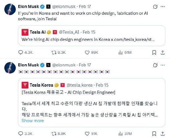
💡Tesla hunts Korean chip talent to rival Nvidia in AI silicon—key for custom infra builders
⚡ 30-Second TL;DR
有什麼變化
埃隆・馬斯克分享特斯拉韓國半導體招聘貼文
為什麼重要
特斯拉的人才招募顯示AI矽晶片的垂直整合加深,可能降低對Nvidia依賴並加速Dojo超級電腦用於自動駕駛。這可能重塑AI基礎設施供應鏈,對建置大規模推論的從業人員影響深遠。
下一步行動
Scan Tesla Korea careers for chip design roles to collaborate on open Dojo hardware specs.
關鍵要點
- •埃隆・馬斯克分享特斯拉韓國半導體招聘貼文
- •鎖定專家以提升內部晶片設計與生產
- •因全球AI晶片市場競爭升溫而驅動
- •屬特斯拉更廣泛AI硬體策略一部分
🧠 深度解析
背景與延伸:來自公開資料,非原文內容。引用 7 個來源。
🔑 增強重點摘要
- •Tesla is establishing a dedicated AI chip design team in South Korea positioned near Samsung's Hwaseong fabrication facilities to accelerate chip development cycles from the traditional 18-24 months to just 9 months[3][5][6]
- •AI5 chip design is nearly complete with initial production builds scheduled for 2026 and major volume ramp in 2027, while AI6 is already in early development stages with both chips manufactured through a dual-foundry strategy using Samsung and TSMC[1][2]
- •Tesla's aggressive recruitment targets world-class semiconductor talent to develop AI chip architecture aimed at achieving the highest production volume in the world, supporting applications across autonomous vehicles, Optimus humanoid robots, and space-based AI computing[3][5][6]
- •The Korea-based team will optimize chip architectures specifically for Tesla's vision-based Full Self-Driving systems and future robotics applications, creating a tighter feedback loop between design and manufacturing[6]
- •Tesla is simultaneously restarting Dojo 3, its third-generation AI training supercomputer, now repositioned for space-based AI compute rather than terrestrial self-driving model training[1][3][4]
📊 競品分析▸ Show
| Aspect | Tesla | Nvidia | Notes |
|---|---|---|---|
| Design Cycle | 9 months (target) | 18-24 months | Tesla pursuing aggressive compression[3][7] |
| Manufacturing | Dual-foundry (Samsung + TSMC) | TSMC primary | Tesla diversifying supply chain[2] |
| Primary Application | In-vehicle inference, robotics | Data center training, inference | Different market focus[1][4] |
| Vertical Integration | High (design + manufacturing partnerships) | Fabless model | Tesla building end-to-end capability[2] |
| Roadmap Transparency | AI4-AI9 detailed publicly | Generational updates less granular | Tesla providing clear technical milestones[3] |
🛠️ 技術深入
• AI5 Specifications: Designed for in-vehicle inference running Full Self-Driving neural networks; targets state-of-the-art performance-per-watt for AI inference with fraction of Nvidia GPU power draw[2] • Manufacturing Strategy: Dual-foundry approach leveraging Samsung's Hwaseong facility and TSMC for parallel production to achieve record-scale volumes[2][5] • Design Methodology: Tesla adopting agile hardware development using advanced electronic design automation (EDA) tools and potentially AI-assisted simulation to compress traditional 18-24 month cycles to 9 months[2][3] • AI6 Specifications: Samsung signed $16.5 billion deal to manufacture AI6 chips at Taylor, Texas fab beginning 2027; designed to power Tesla vehicles, Optimus robots, and enable high-performance AI training in data centers[4] • Dojo 3 Architecture: Restarted training supercomputer now optimized for space-based AI compute infrastructure rather than terrestrial autonomous driving model training[3][4] • Multi-Processor Roadmap: AI5 and AI6 represent milestones in broader roadmap extending to AI7, AI8, and AI9 with nine-month generational cycles, supporting in-vehicle autonomy, robotics processors, and training silicon[2][3]
🔮 前景展望AI analysis grounded in cited sources
Tesla's Korea-based recruitment and accelerated chip design cycles position the company to achieve unprecedented vertical integration in AI silicon, potentially reducing dependency on external chip suppliers and enabling tighter control over autonomous vehicle and robotics performance trajectories. The dual-foundry strategy and aggressive 9-month design cadence could establish new industry benchmarks for AI chip development velocity, forcing competitors to reconsider traditional 18-24 month cycles. Success in space-based AI compute via Dojo 3 would expand Tesla's addressable market beyond automotive and robotics into infrastructure computing. However, the realistic near-term outcome may involve hybrid approaches where Tesla expands internal capability while leveraging established compute ecosystems for frontier-model training[1]. For the broader AI chip market, Tesla's vertical integration strategy challenges the fabless model dominance and could inspire other automotive and robotics companies to develop proprietary silicon, fragmenting the market away from Nvidia's current dominance in AI inference and training.
⏳ 時間線
📎 來源 (7)
Factual claims are grounded in the sources below. Forward-looking analysis is AI-generated interpretation.
- heygotrade.com — Musk Signals Teslas AI Chips Are Near Ready As Dojo 3 Returns to the Game
- futurumgroup.com — Is Teslas Multi Foundry Strategy the Blueprint for Record AI Chip Volumes
- tesery.com — Tesla Resumes Dojo 3 Development As Ai5 Chip Design Stabilizes
- TechCrunch — Elon Musk Says Teslas Restarted Dojo3 Will Be for Space Based AI Compute
- basenor.com — Tesla Expands AI Chip Team in South Korea What It Means
- teslanorth.com — Tesla Expands Next Gen AI Chip Design Into South Korea
- datacenterdynamics.com — Elon Musk Says Tesla Is Aiming for a Nine Month Chip Design Cadence Will Resurrect Its Dojo Chip Project
AI 週報
閱讀本週精選 AI 大事摘要 →
👉相關動態
AI 策展新聞聚合。所有內容版權歸原始發布者所有。
原始來源: cnBeta (Full RSS) ↗
每週 AI 簡報
每週一封,可隨時退訂。