來源cnBeta (Full RSS)•較早收集於 57m
英特爾18A-P關鍵數據:功耗降18% 性能升9%
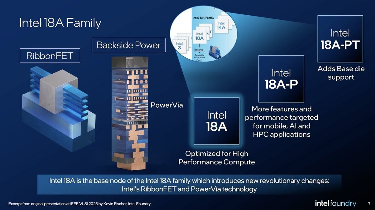
英特爾18A-P功耗降18%—降低下一代晶片AI資料中心成本。(32字元)
30 秒速覽
有什麼變化
於夏威夷VLSI 2026透過T1.2論文公布
為什麼重要
提升英特爾AI加速器及資料中心晶片的省電前景。可降低大規模AI訓練與推論部署的營運成本。
下一步行動
在AI硬體規劃中基準測試英特爾18A路線圖,以獲取潛在18%省電。
誰應關注:Enterprise & Security Teams
關鍵要點
- •於夏威夷VLSI 2026透過T1.2論文公布
- •同功耗下性能提升超過9%(相較18A)
- •同性能下功耗降低超過18%
- •針對先進節點提升效率
關鍵數字9%18%
深度解析
本篇為 AI 生成分析,非原文內容。
增強重點摘要
- •The 18A-P node utilizes an optimized backside power delivery network (BSPDN) implementation, specifically refining the PowerVia interconnect density to reduce IR drop compared to the base 18A process.
- •Intel's T1.2 paper indicates that 18A-P achieves these gains through a combination of improved standard cell library scaling and the integration of new high-k metal gate (HKMG) materials to reduce leakage current.
- •The 18A-P process is positioned as a 'performance-optimized' variant intended primarily for high-end compute and AI accelerator workloads, rather than a general-purpose replacement for the standard 18A node.
競品分析
Primary Advantage
- Intel 18A-P
- Backside Power Delivery (PowerVia)
- TSMC N2P
- Mature Ecosystem/Yield
- Samsung 2nm (SF2)
- GAAFET Maturity
Performance Gain
- Intel 18A-P
9% vs 18A
- TSMC N2P
- ~5-10% vs N2
- Samsung 2nm (SF2)
- ~12% vs 3nm
Power Reduction
- Intel 18A-P
18% vs 18A
- TSMC N2P
- ~15% vs N2
- Samsung 2nm (SF2)
- ~25% vs 3nm
| Feature | Intel 18A-P | TSMC N2P | Samsung 2nm (SF2) |
|---|---|---|---|
| Primary Advantage | Backside Power Delivery (PowerVia) | Mature Ecosystem/Yield | GAAFET Maturity |
| Performance Gain | 9% vs 18A | ~5-10% vs N2 | ~12% vs 3nm |
| Power Reduction | 18% vs 18A | ~15% vs N2 | ~25% vs 3nm |
技術深入
- Backside Power Delivery (PowerVia): 18A-P refines the PowerVia architecture by optimizing the via-to-metal pitch, which significantly lowers resistance in the power delivery network.
- Standard Cell Optimization: The process node introduces a new 5.5-track (5.5T) standard cell library, allowing for higher logic density and reduced parasitic capacitance.
- Material Science: Implementation of advanced barrier materials in the interconnect stack to mitigate electromigration at higher current densities.
- Design Rule Manual (DRM): 18A-P features tighter design rules for local interconnects, facilitating the performance boost at the same power envelope.
前景展望基於引用來源的 AI 分析
Intel will prioritize 18A-P for its internal AI accelerator roadmap.
The performance-per-watt profile of 18A-P directly addresses the thermal and power constraints of high-density AI silicon.
Foundry customers will see a bifurcated pricing model for 18A and 18A-P.
The additional process steps required for 18A-P optimization will necessitate a premium pricing structure compared to the standard 18A node.
時間線
2021-07
Intel announces PowerVia and RibbonFET technology as part of the IDM 2.0 strategy.
2023-09
Intel confirms the 18A process node is on track for high-volume manufacturing.
2024-02
Intel Foundry Services (IFS) rebrands to Intel Foundry and details the 18A roadmap.
2025-06
Intel begins initial risk production of the base 18A process node.
2026-04
Intel presents the 18A-P process node at the VLSI 2026 symposium.
- 2021-07Intel announces PowerVia and RibbonFET technology as part of the IDM 2.0 strategy.
- 2023-09Intel confirms the 18A process node is on track for high-volume manufacturing.
- 2024-02Intel Foundry Services (IFS) rebrands to Intel Foundry and details the 18A roadmap.
- 2025-06Intel begins initial risk production of the base 18A process node.
- 2026-04Intel presents the 18A-P process node at the VLSI 2026 symposium.
AI 週報
閱讀本週精選 AI 大事摘要 →
相關動態

AI 策展新聞聚合。所有內容版權歸原始發布者所有。
原始來源: cnBeta (Full RSS) ↗
每週電子報
每週一封,可隨時退訂。