🇨🇳cnBeta (Full RSS)•Stalecollected in 57m
Intel 18A-P: 18% Power Cut, 9% Perf Boost
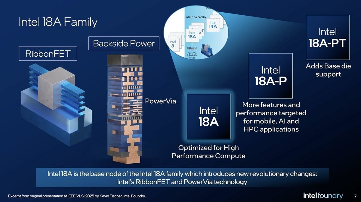
💡Intel 18A-P's 18% power drop slashes AI data center costs on next-gen chips.
⚡ 30-Second TL;DR
What Changed
Announced at VLSI 2026 in Hawaii via T1.2 paper
Why It Matters
Boosts prospects for power-efficient AI accelerators and data center chips from Intel. Could reduce operational costs for large-scale AI training and inference deployments.
What To Do Next
Benchmark Intel 18A roadmaps in your AI hardware planning for potential 18% power savings.
Who should care:Enterprise & Security Teams
Key Points
- •Announced at VLSI 2026 in Hawaii via T1.2 paper
- •>9% performance increase at identical power vs 18A
- •>18% power reduction at same performance level
- •Targets enhanced efficiency for advanced nodes
🧠 Deep Insight
AI-generated analysis for this event.
🔑 Enhanced Key Takeaways
- •The 18A-P node utilizes an optimized backside power delivery network (BSPDN) implementation, specifically refining the PowerVia interconnect density to reduce IR drop compared to the base 18A process.
- •Intel's T1.2 paper indicates that 18A-P achieves these gains through a combination of improved standard cell library scaling and the integration of new high-k metal gate (HKMG) materials to reduce leakage current.
- •The 18A-P process is positioned as a 'performance-optimized' variant intended primarily for high-end compute and AI accelerator workloads, rather than a general-purpose replacement for the standard 18A node.
📊 Competitor Analysis▸ Show
| Feature | Intel 18A-P | TSMC N2P | Samsung 2nm (SF2) |
|---|---|---|---|
| Primary Advantage | Backside Power Delivery (PowerVia) | Mature Ecosystem/Yield | GAAFET Maturity |
| Performance Gain | >9% vs 18A | ~5-10% vs N2 | ~12% vs 3nm |
| Power Reduction | >18% vs 18A | ~15% vs N2 | ~25% vs 3nm |
🛠️ Technical Deep Dive
- Backside Power Delivery (PowerVia): 18A-P refines the PowerVia architecture by optimizing the via-to-metal pitch, which significantly lowers resistance in the power delivery network.
- Standard Cell Optimization: The process node introduces a new 5.5-track (5.5T) standard cell library, allowing for higher logic density and reduced parasitic capacitance.
- Material Science: Implementation of advanced barrier materials in the interconnect stack to mitigate electromigration at higher current densities.
- Design Rule Manual (DRM): 18A-P features tighter design rules for local interconnects, facilitating the performance boost at the same power envelope.
🔮 Future ImplicationsAI analysis grounded in cited sources
Intel will prioritize 18A-P for its internal AI accelerator roadmap.
The performance-per-watt profile of 18A-P directly addresses the thermal and power constraints of high-density AI silicon.
Foundry customers will see a bifurcated pricing model for 18A and 18A-P.
The additional process steps required for 18A-P optimization will necessitate a premium pricing structure compared to the standard 18A node.
⏳ Timeline
2021-07
Intel announces PowerVia and RibbonFET technology as part of the IDM 2.0 strategy.
2023-09
Intel confirms the 18A process node is on track for high-volume manufacturing.
2024-02
Intel Foundry Services (IFS) rebrands to Intel Foundry and details the 18A roadmap.
2025-06
Intel begins initial risk production of the base 18A process node.
2026-04
Intel presents the 18A-P process node at the VLSI 2026 symposium.
📰
Weekly AI Recap
Read this week's curated digest of top AI events →
👉Related Updates
Same topic
Explore #process-node
Same product
More on intel-18a-p
Same source
Latest from cnBeta (Full RSS)

PACA: Open-source tool for ancient fossil coordinate mapping
cnBeta (Full RSS)•Jul 28

First atmosphere detected on habitable-zone exoplanet
cnBeta (Full RSS)•Jul 25

Samsung Secures $200B Broadcom AI Infrastructure Deal
cnBeta (Full RSS)•Jul 25

How AMD's 2006 ATI Acquisition Built Today's AI Empire
cnBeta (Full RSS)•Jul 25
AI-curated news aggregator. All content rights belong to original publishers.
Original source: cnBeta (Full RSS) ↗