Xuanjie O100 Drops Camera for AI Power
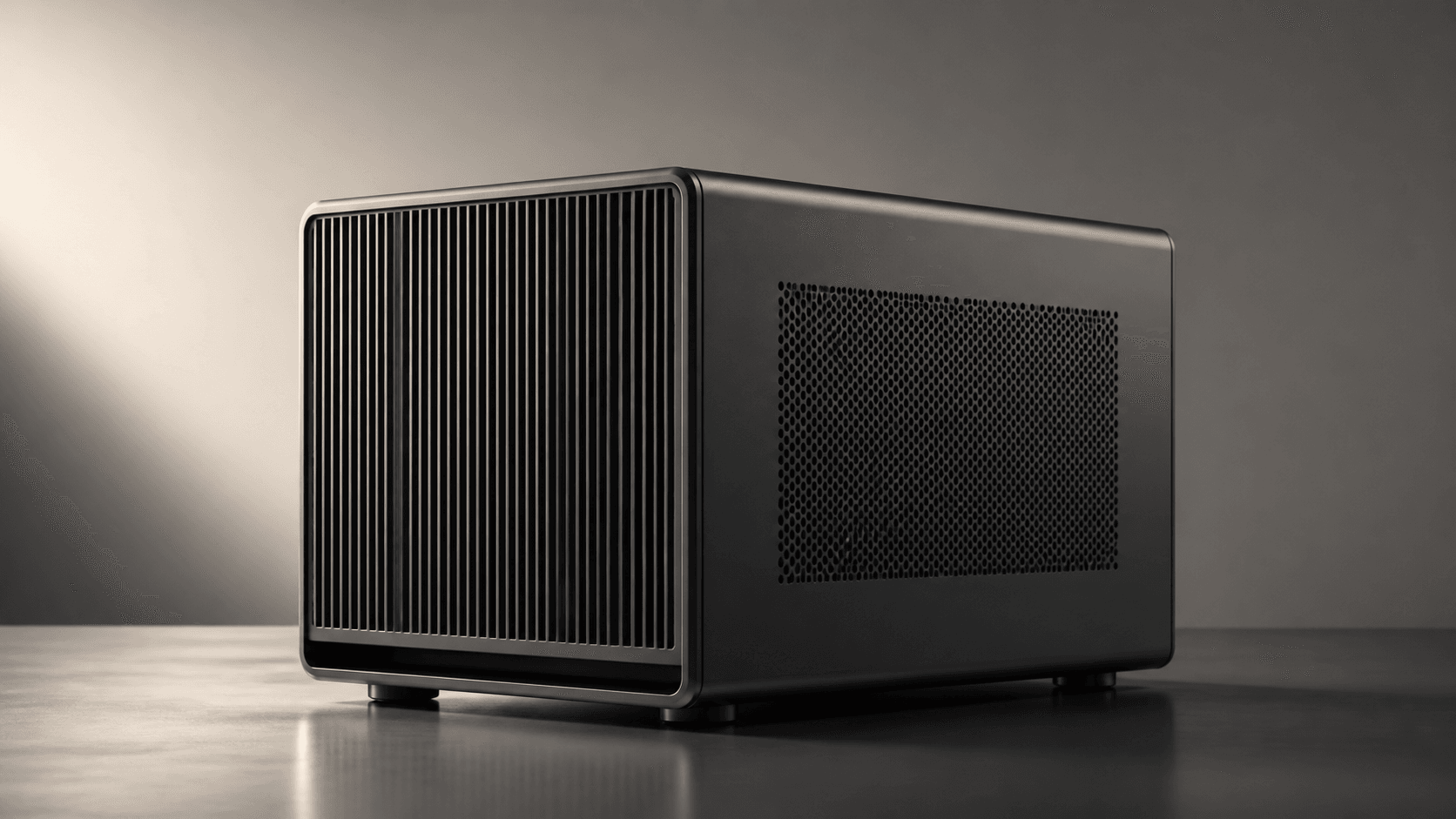
💡A camera-free Xiaomi prototype reveals how much hardware design may change for fast, local AI inference.
⚡ 30-Second TL;DR
What Changed
The Xuanjie O100 is an on-device AI terminal prototype from Xiaomi.
Why It Matters
The prototype signals a product direction that prioritizes local AI inference over conventional smartphone hardware features. If the reported throughput is representative, it could encourage developers to consider dedicated cooling and heterogeneous compute designs for edge AI products.
What To Do Next
Benchmark MiMo at comparable token-generation workloads on your target edge hardware, recording throughput, power draw, and sustained thermal performance.
Key Points
- •The Xuanjie O100 is an on-device AI terminal prototype from Xiaomi.
- •It removes the rear camera and prioritizes dual-chip computing.
- •Active air-cooling supports MiMo inference at about 295 tokens per second.
🧠 Deep Insight
Background and context from public sources — not the original article. 12 sources cited.
🔑 Enhanced Key Takeaways
- •The Xuanjie O100 utilizes a 6nm process node integrated with wafer-level vertical stacking (Wafer on Wafer) and Hybrid Bonding technology featuring a 1.4-micrometer pitch.
- •The chip achieves a memory bandwidth of 1.22 TB/s, which is 16 times higher than standard flagship smartphone SoCs.
- •The O100 is part of a broader three-chip ecosystem strategy, alongside the Xuanjie O3 flagship SoC and the Xuanjie D100 intelligent driving chip.
- •While the O100 prototype reached 295 tokens per second in the terminal, the standalone chip has demonstrated peak edge-side inference speeds of up to 330 tokens per second.
- •The Xuanjie O100 is currently in the prototype phase with a scheduled commercial rollout targeted for 2027, distinct from the O3 chip slated for the Xiaomi 18 Fold.
📊 Competitor Analysis▸ Show
| Feature | Xuanjie O100 (Prototype) | Standard Flagship SoC (2026) |
|---|---|---|
| Memory Bandwidth | 1.22 TB/s | ~0.07-0.08 TB/s |
| Primary Focus | Dedicated AI Inference | General Purpose Computing |
| Cooling | Active Air-Cooling | Passive/Vapor Chamber |
| Camera Integration | None (Removed) | Integrated ISP |
🛠️ Technical Deep Dive
- Architecture: Dedicated high-bandwidth AI acceleration chip for edge-side large model inference.
- Process Node: 6nm manufacturing process.
- Packaging: Wafer-level vertical stacking (Wafer on Wafer) with Hybrid Bonding.
- Bonding Pitch: 1.4-micrometer.
- Memory Bandwidth: 1.22 TB/s.
- Thermal Management: Active air-cooling system integrated into the terminal prototype.
- Computing Configuration: Dual-chip architecture combining the O3 AI flagship SoC and the O100 accelerator.
🔮 Future ImplicationsAI analysis grounded in cited sources
⏳ Timeline
📎 Sources (12)
Factual claims are grounded in the sources below. Forward-looking analysis is AI-generated interpretation.
Weekly AI Recap
Read this week's curated digest of top AI events →
👉Related Updates

AI-curated news aggregator. All content rights belong to original publishers.
Original source: Pandaily ↗
This is a summary, not the original. Read the source, or get the weekly briefing.
Weekly AI briefing
One email a week. Unsubscribe anytime.