TSMC Secures Land for 1.4nm Expansion
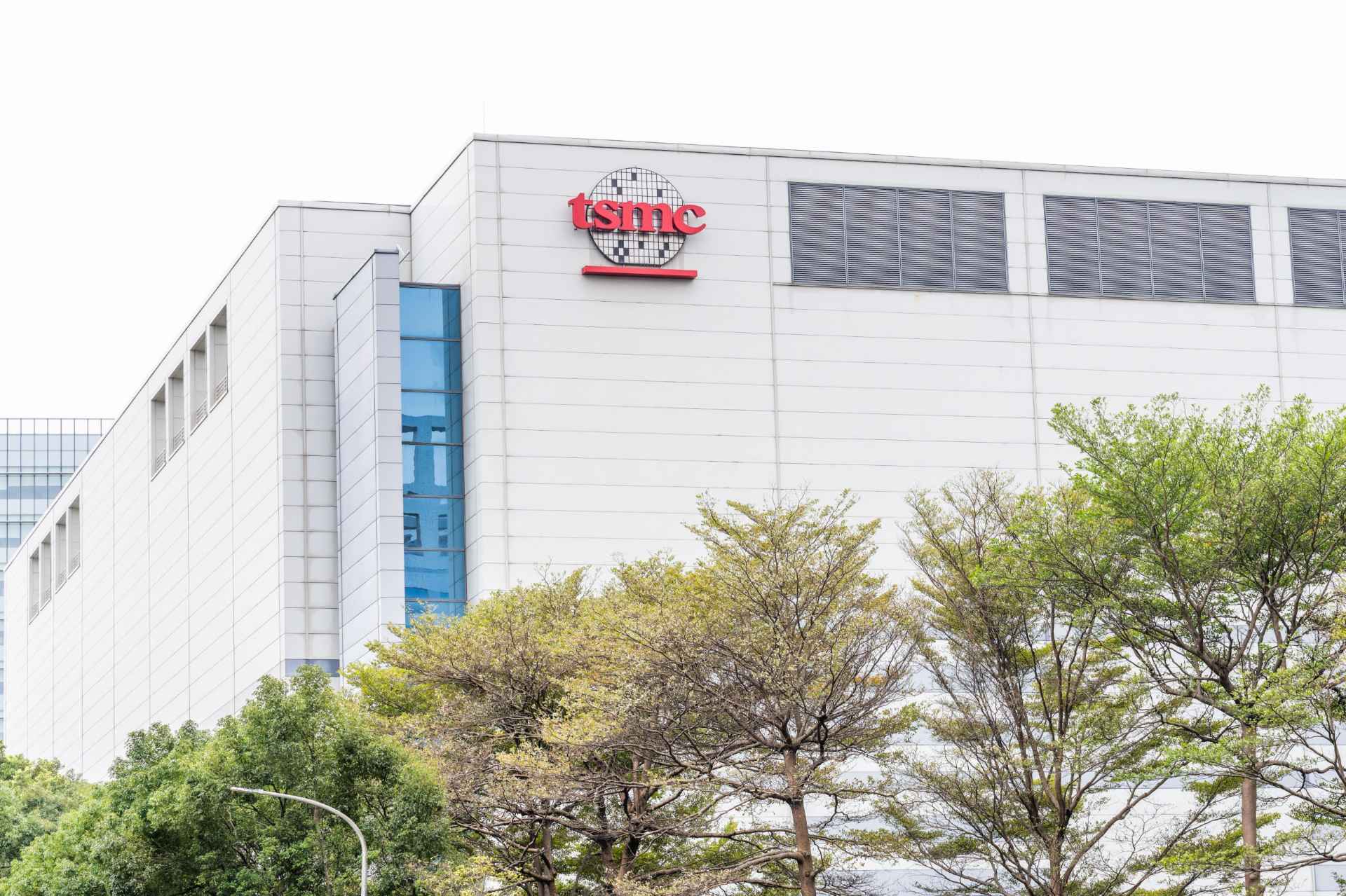
TSMC may add two 1.4nm fabs and advanced packaging capacity—critical for future AI chips.
30-Second TL;DR
What Changed
TSMC's domestic Taiwan expansion has overcome a major land-acquisition obstacle.
Why It Matters
The expansion could strengthen Taiwan's capacity for producing advanced chips used in AI accelerators and high-performance computing. Combining leading-edge fabrication with advanced packaging may also improve TSMC's ability to support increasingly complex AI systems.
What To Do Next
Review your AI hardware roadmap and supplier assumptions for 1.4nm availability and advanced packaging capacity from TSMC.
Key Points
- •TSMC's domestic Taiwan expansion has overcome a major land-acquisition obstacle.
- •The plan includes two 1.4nm wafer foundries.
- •A panel-level advanced packaging facility is also planned at the site.
Deep Insight
AI-generated analysis for this event — not the original article.
Enhanced Key Takeaways
- •The expansion site is located in the Hsinchu Science Park's Baoshan Phase 2 expansion area, which has been the primary focus for TSMC's most advanced node development.
- •The transition to 1.4nm, often referred to as the A14 node, is expected to utilize High-NA EUV lithography tools to manage the extreme scaling requirements.
- •Local opposition was primarily driven by land compensation disputes and environmental impact concerns regarding water and electricity consumption in the Hsinchu region.
- •Panel-level packaging (PLP) is a strategic shift for TSMC to increase throughput and reduce costs compared to traditional wafer-level packaging (CoWoS) for AI accelerators.
- •The Taiwanese government has played a direct role in mediating these land disputes to ensure TSMC maintains its 'Silicon Shield' strategy amidst global semiconductor competition.
Competitor Analysis
- TSMC (A14/1.4nm)
- Land secured/Development
- Intel (14A)
- In development
- Samsung (SF1.4)
- In development
- TSMC (A14/1.4nm)
- High-NA EUV
- Intel (14A)
- High-NA EUV
- Samsung (SF1.4)
- High-NA EUV
- TSMC (A14/1.4nm)
- Integrated PLP/CoWoS
- Intel (14A)
- Foveros/EMIB
- Samsung (SF1.4)
- I-Cube/SAINT
| Feature | TSMC (A14/1.4nm) | Intel (14A) | Samsung (SF1.4) |
|---|---|---|---|
| Status | Land secured/Development | In development | In development |
| Lithography | High-NA EUV | High-NA EUV | High-NA EUV |
| Packaging | Integrated PLP/CoWoS | Foveros/EMIB | I-Cube/SAINT |
Technical Deep Dive
- A14 (1.4nm) node utilizes Gate-All-Around (GAA) nanosheet transistor architecture to improve electrostatic control and drive current.
- Panel-level packaging involves processing chips on large rectangular panels rather than circular wafers, significantly increasing the surface area available for packaging and reducing edge waste.
- High-NA EUV (0.55 numerical aperture) is required to achieve the resolution necessary for 1.4nm features, necessitating a shift from 0.33 NA EUV systems.
- The process node is designed to optimize power-performance-area (PPA) specifically for high-bandwidth memory (HBM) integration and massive AI compute clusters.
Future ImplicationsAI analysis grounded in cited sources
Timeline
- 2022-06TSMC officially announces development of the 1.4nm node (A14).
- 2023-09Hsinchu Science Park Baoshan Phase 2 expansion faces significant protests from local landowners.
- 2024-04TSMC confirms plans to integrate advanced packaging capacity into its Hsinchu expansion sites.
- 2025-11Government mediation efforts intensify to resolve land acquisition deadlocks for semiconductor infrastructure.
- 2026-07Final agreements reached with landowners, clearing the path for construction.
Weekly AI Recap
Read this week's curated digest of top AI events →
Related Updates


AI-curated news aggregator. All content rights belong to original publishers.
Original source: cnBeta (Full RSS) ↗
This is a summary, not the original. Read the source, or get the weekly briefing.
The weekly digest
One email a week. Unsubscribe anytime.