The brutal economics of the global memory chip war
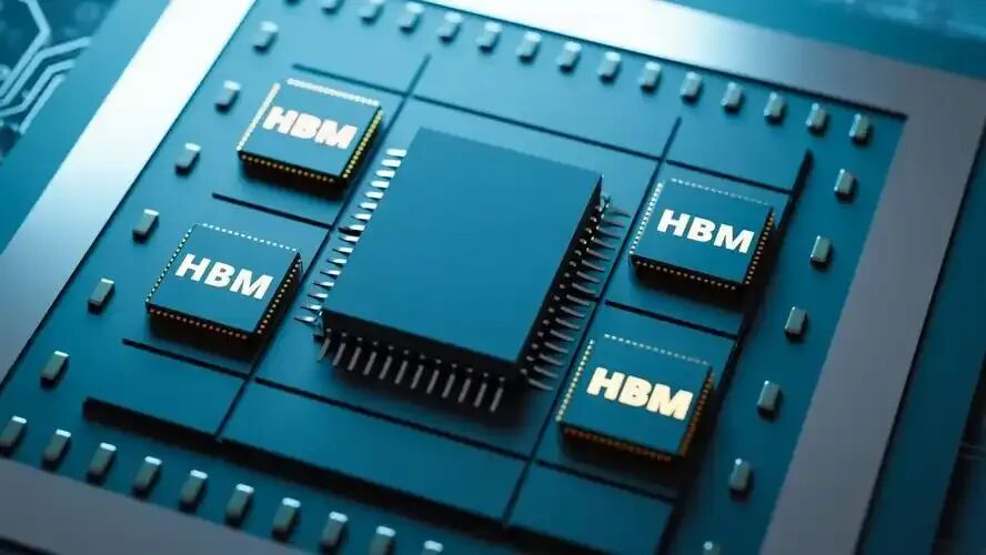
💡HBM is the bottleneck for AI training; understanding the memory industry's brutal history explains current GPU pricing.
⚡ 30-Second TL;DR
What Changed
The DRAM market is now dominated by Samsung, SK Hynix, and Micron, controlling over 90% of global capacity.
Why It Matters
Understanding the memory chip supply chain is critical for AI practitioners, as HBM (High Bandwidth Memory) availability directly impacts AI hardware and training costs.
What To Do Next
Factor in DRAM/HBM supply chain volatility when planning large-scale GPU cluster deployments or long-term AI infrastructure budgets.
Key Points
- •The DRAM market is now dominated by Samsung, SK Hynix, and Micron, controlling over 90% of global capacity.
- •Historical survival in this industry required massive, counter-cyclical investments during downturns.
- •Geopolitical tensions and export controls are creating new fractures in the previously consolidated memory market.
🧠 Deep Insight
AI-generated analysis for this event — not the original article.
🔑 Enhanced Key Takeaways
- •The rise of High Bandwidth Memory (HBM) has fundamentally altered DRAM economics, shifting focus from commodity volume to high-margin, AI-specific architectures.
- •Chinese memory manufacturers, specifically CXMT (ChangXin Memory Technologies), are rapidly increasing domestic capacity to mitigate the impact of US-led export restrictions on advanced lithography equipment.
- •The transition from planar DRAM to 3D DRAM architectures is currently the primary R&D battleground, as scaling limits for traditional 2D structures have been reached at the 10nm node.
- •Memory manufacturers are increasingly integrating 'Processing-in-Memory' (PIM) technologies to alleviate the von Neumann bottleneck in AI training and inference workloads.
- •Supply chain diversification is forcing a shift from 'Just-in-Time' to 'Just-in-Case' inventory models, increasing the capital intensity required for regionalized manufacturing hubs.
📊 Competitor Analysis▸ Show
| Feature | Samsung | SK Hynix | Micron |
|---|---|---|---|
| Primary HBM Strategy | HBM3E / HBM4 | HBM3E (Market Leader) | HBM3E (High Capacity) |
| Process Node | 12nm-class DRAM | 10nm-class (1a/1b) | 1-beta / 1-gamma |
| Market Focus | Consumer/Enterprise | AI/Data Center | Enterprise/Cloud |
🛠️ Technical Deep Dive
- HBM3E Architecture: Utilizes TSV (Throughput Silicon Via) technology to stack DRAM dies vertically, achieving bandwidths exceeding 1 TB/s per stack.
- 3D DRAM Implementation: Moving away from capacitor-on-bitline structures to vertical channel transistors to enable scaling beyond the 10nm limit.
- EUV Lithography: Adoption of Extreme Ultraviolet lithography is now mandatory for sub-14nm DRAM layers to maintain yield rates and reduce multi-patterning complexity.
- PIM (Processing-in-Memory): Integration of logic units directly into the DRAM die to perform MAC (Multiply-Accumulate) operations, reducing data movement energy consumption by up to 70%.
🔮 Future ImplicationsAI analysis grounded in cited sources
⏳ Timeline
Weekly AI Recap
Read this week's curated digest of top AI events →
👉Related Updates


AI-curated news aggregator. All content rights belong to original publishers.
Original source: 虎嗅 ↗
This is a summary, not the original. Read the source, or get the weekly briefing.
The weekly digest
One email a week. Unsubscribe anytime.