Tesla’s Terafab Gets Its Manufacturing Architect
Tesla is moving from designing AI chips to controlling the fabs that manufacture them.
30-Second TL;DR
What Changed
Terafab will receive an initial investment of $16.8 billion and serve as a computing manufacturing base for Tesla and SpaceX.
Why It Matters
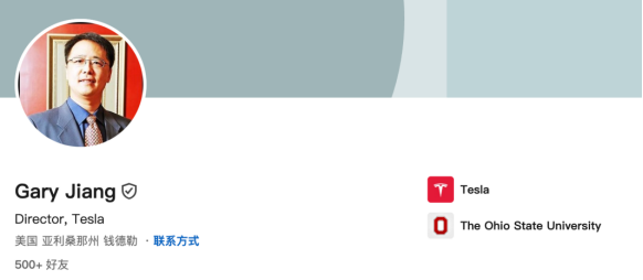
Terafab could give Musk’s companies greater control over the supply and production of AI chips, but building a competitive advanced fab requires years of process, yield, and equipment expertise. Gary Jiang’s appointment suggests Tesla is prioritizing manufacturing execution and closer integration with Intel rather than relying solely on external foundries.
What To Do Next
Map your AI hardware roadmap against Intel 14A, Samsung, and TSMC supply options before committing to custom accelerator deployments.
Key Points
- •Terafab will receive an initial investment of $16.8 billion and serve as a computing manufacturing base for Tesla and SpaceX.
- •Gary Jiang brings experience in Intel fab construction, technology transfer, equipment installation, process management, and mass-production readiness.
- •Intel is reportedly supporting Terafab, with the factory expected to use Intel’s next-generation 14A process.
- •Tesla’s move follows the shutdown of the Dojo team and increased reliance on Samsung and TSMC for chip manufacturing.
Deep Insight
AI-generated analysis for this event — not the original article.
Enhanced Key Takeaways
- •The Terafab facility is strategically located near Tesla's Gigafactory Texas to minimize latency in data transfer and supply chain logistics for AI hardware integration.
- •Gary Jiang's appointment is part of a broader 'Project Titan' initiative at Tesla, aimed at vertical integration of silicon manufacturing to reduce dependency on external foundry capacity constraints.
- •Intel's involvement in Terafab includes a technology licensing agreement that allows Tesla to utilize proprietary 14A lithography techniques for custom AI accelerator production.
- •The $16.8 billion investment is structured as a joint venture between Tesla and SpaceX, with SpaceX providing the primary demand for high-performance computing (HPC) chips for Starlink and Starship AI systems.
- •Industry analysts suggest the shift away from the internal Dojo team's custom architecture toward standard 14A process nodes indicates a pivot toward more scalable, industry-standard software compatibility.
Competitor Analysis
- Tesla Terafab
- Internal AI/Robotics
- TSMC (N2/A16)
- External Foundry/HPC
- Samsung Foundry (SF2)
- External Foundry/Mobile
- Tesla Terafab
- Intel 14A (Custom)
- TSMC (N2/A16)
- 2nm / 1.6nm
- Samsung Foundry (SF2)
- 2nm (GAA)
- Tesla Terafab
- High (Full Stack)
- TSMC (N2/A16)
- Low (Foundry Only)
- Samsung Foundry (SF2)
- Medium (Memory/Logic)
| Feature | Tesla Terafab | TSMC (N2/A16) | Samsung Foundry (SF2) |
|---|---|---|---|
| Primary Focus | Internal AI/Robotics | External Foundry/HPC | External Foundry/Mobile |
| Process Node | Intel 14A (Custom) | 2nm / 1.6nm | 2nm (GAA) |
| Vertical Integration | High (Full Stack) | Low (Foundry Only) | Medium (Memory/Logic) |
Technical Deep Dive
- Terafab utilizes Intel 14A (1.4nm class) process technology, which leverages High-NA EUV lithography for increased transistor density.
- The facility is designed for heterogeneous integration, utilizing advanced packaging techniques such as 3D Foveros to stack logic and memory dies.
- Power delivery systems at the fab are optimized for high-TDP (Thermal Design Power) AI chips, incorporating liquid cooling infrastructure directly into the manufacturing floor.
- The architecture supports chiplet-based designs, allowing Tesla to mix and match compute tiles for different applications ranging from autonomous driving (FSD) to humanoid robotics (Optimus).
Future ImplicationsAI analysis grounded in cited sources
Timeline
- 2024-06Tesla announces the expansion of the Austin computing cluster to support massive AI training.
- 2025-03Tesla officially shutters the internal Dojo custom-silicon team to pivot toward industry-standard nodes.
- 2025-11Tesla and SpaceX sign a memorandum of understanding for a joint-venture semiconductor manufacturing facility.
- 2026-07Gary Jiang is appointed as the lead manufacturing architect for the Terafab project.
Weekly AI Recap
Read this week's curated digest of top AI events →
AI-curated news aggregator. All content rights belong to original publishers.
Original source: 虎嗅 ↗
This is a summary, not the original. Read the source, or get the weekly briefing.
The weekly digest
One email a week. Unsubscribe anytime.