SK Hynix Warns of Memory Shortage Through 2030
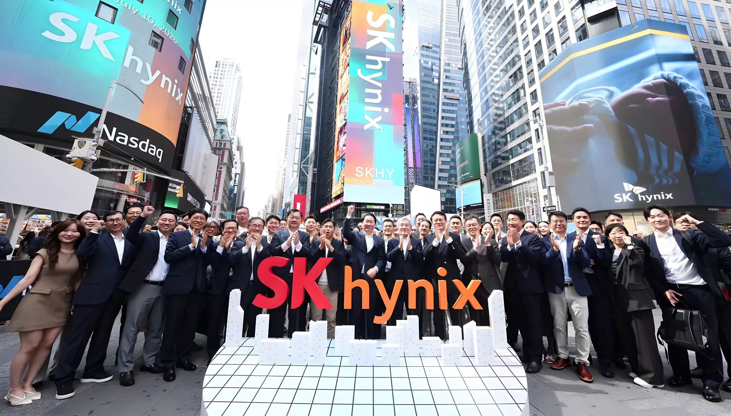
💡Critical supply chain news: Memory shortages could impact AI scaling and hardware costs for years to come.
⚡ 30-Second TL;DR
What Changed
2027 is projected to be the most difficult year for memory supply.
Why It Matters
Persistent memory shortages could significantly increase costs for AI model training and data center infrastructure deployment.
What To Do Next
Review your infrastructure procurement strategy to account for long-term memory supply volatility.
Key Points
- •2027 is projected to be the most difficult year for memory supply.
- •Global demand for memory chips continues to outpace production capacity.
- •Supply chain constraints are expected to last until 2030.
🧠 Deep Insight
AI-generated analysis for this event — not the original article.
🔑 Enhanced Key Takeaways
- •The surge in demand is primarily driven by the rapid integration of high-bandwidth memory (HBM) in AI accelerators and large-scale data center infrastructure.
- •SK Hynix has committed to massive capital expenditure increases, including the construction of new fabrication plants in South Korea and the United States to address the bottleneck.
- •The industry is experiencing a transition toward 'customized' memory solutions, where chip architecture is increasingly tailored to specific AI workloads rather than standardized commodity DRAM.
- •Energy consumption and thermal management challenges in high-density memory stacks are forcing a shift in manufacturing processes, such as advanced packaging techniques like MR-MUF.
- •Geopolitical trade restrictions and export controls on semiconductor manufacturing equipment have complicated the ability of memory manufacturers to scale production capacity globally.
📊 Competitor Analysis▸ Show
| Feature | SK Hynix | Samsung Electronics | Micron Technology |
|---|---|---|---|
| HBM Market Position | Leader (HBM3E/HBM4) | Strong Challenger | Emerging Competitor |
| Primary Strategy | AI-focused capacity expansion | Diversified memory/foundry | High-margin HBM/DDR5 focus |
| Recent Tech Milestone | 12-layer HBM3E mass production | 12-layer HBM3E development | HBM3E volume production |
🛠️ Technical Deep Dive
- HBM3E Architecture: Utilizes 12-layer stacking technology to achieve higher bandwidth and capacity per die compared to previous generations.
- MR-MUF (Mass Reflow Molded Underfill): A proprietary packaging technique used by SK Hynix to improve thermal dissipation and yield rates in high-stack memory modules.
- Through-Silicon Vias (TSV): Essential interconnect technology allowing vertical stacking of DRAM dies to minimize latency and power consumption.
- HBM4 Transition: Industry shift toward 2048-bit wide interfaces, doubling the bus width of HBM3E to support next-generation AI compute requirements.
🔮 Future ImplicationsAI analysis grounded in cited sources
⏳ Timeline
Weekly AI Recap
Read this week's curated digest of top AI events →
👉Related Updates
AI-curated news aggregator. All content rights belong to original publishers.
Original source: cnBeta (Full RSS) ↗
This is a summary, not the original. Read the source, or get the weekly briefing.
The weekly digest
One email a week. Unsubscribe anytime.