Samsung Taylor Fab Nears Production
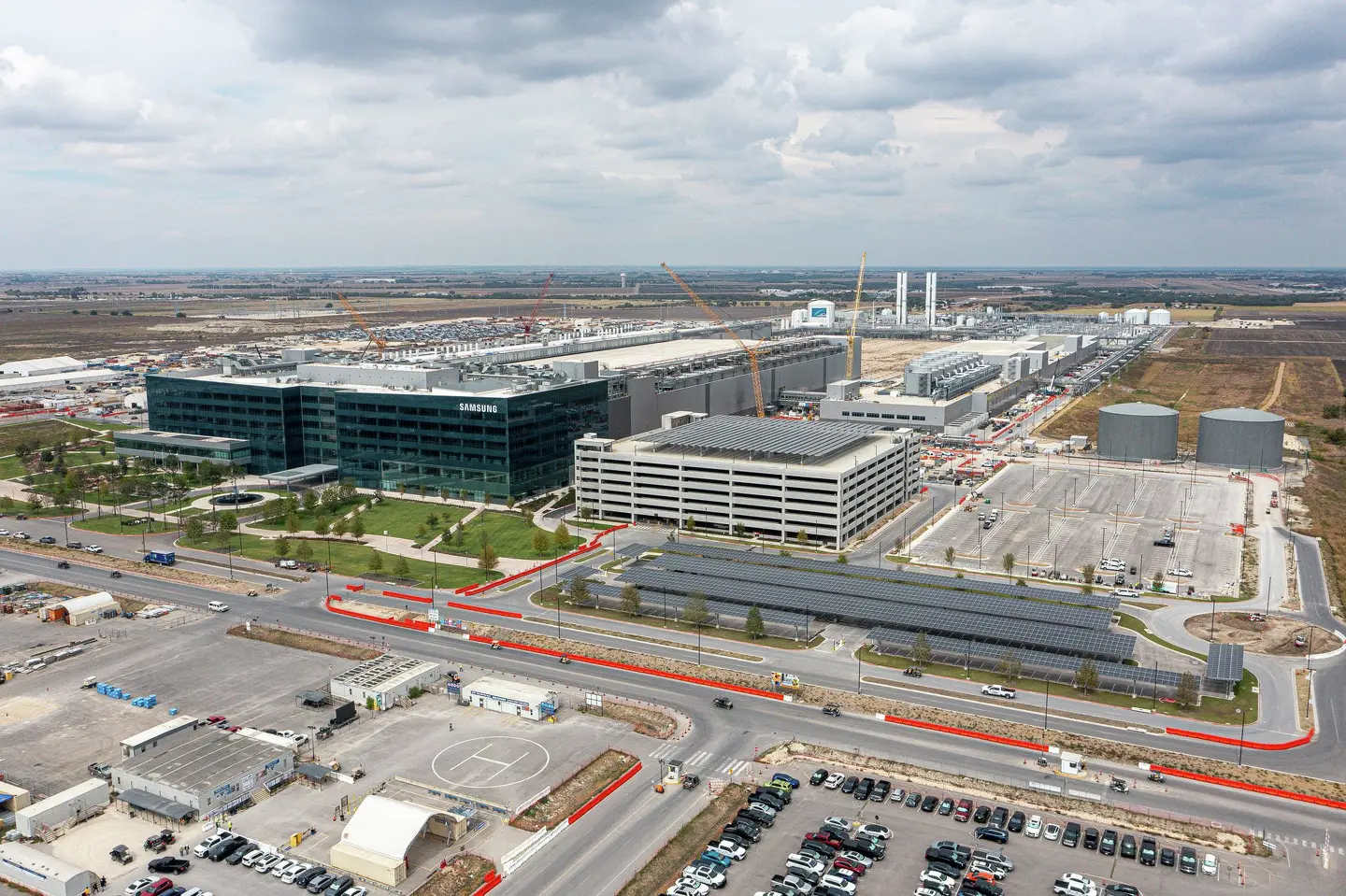
Samsung’s new US foundry may reshape supply options for future AI chips.
30-Second TL;DR
What Changed
Samsung has opened recruitment for next summer’s internship program at the Taylor facility.
Why It Matters
The factory’s start-up could expand US-based semiconductor manufacturing capacity and potentially diversify supply options for AI chip companies. Its production timeline will be relevant to organizations planning future accelerator and custom silicon programs.
What To Do Next
Track Samsung’s Taylor foundry production updates and assess whether its future capacity could support your AI accelerator or custom-silicon roadmap.
Key Points
- •Samsung has opened recruitment for next summer’s internship program at the Taylor facility.
- •The Taylor site is being included in Samsung’s global internship program for the first time.
- •The advanced foundry is scheduled to begin production by the end of this year.
Deep Insight
AI-generated analysis for this event — not the original article.
Enhanced Key Takeaways
- •The Taylor, Texas facility is part of a massive $40 billion-plus investment strategy supported by the U.S. CHIPS and Science Act, which includes significant federal grant funding.
- •Samsung's Taylor site is designed to utilize advanced process nodes, specifically targeting 4nm and 2nm fabrication capabilities to compete for high-performance computing and AI chip contracts.
- •The project has faced multiple timeline adjustments, with initial production targets originally set for 2024 before being pushed back to 2026 due to market conditions and construction complexities.
- •The facility is expected to include a dedicated advanced packaging line, allowing Samsung to offer end-to-end manufacturing services for U.S.-based fabless semiconductor companies.
- •Samsung is coordinating with local Texas educational institutions, such as the University of Texas at Austin, to build a specialized talent pipeline for the semiconductor workforce.
Competitor Analysis
- Samsung (Taylor)
- 4nm / 2nm
- TSMC (Arizona)
- 4nm / 3nm / 2nm
- Intel (Foundry)
- 18A / 14A
- Samsung (Taylor)
- Advanced Foundry
- TSMC (Arizona)
- Advanced Foundry
- Intel (Foundry)
- IDM 2.0 / Foundry
- Samsung (Taylor)
- Nearing Production
- TSMC (Arizona)
- Production (Fab 21)
- Intel (Foundry)
- Scaling 18A
| Feature | Samsung (Taylor) | TSMC (Arizona) | Intel (Foundry) |
|---|---|---|---|
| Primary Node Focus | 4nm / 2nm | 4nm / 3nm / 2nm | 18A / 14A |
| U.S. Strategy | Advanced Foundry | Advanced Foundry | IDM 2.0 / Foundry |
| Status (2026) | Nearing Production | Production (Fab 21) | Scaling 18A |
Technical Deep Dive
- The Taylor facility utilizes Extreme Ultraviolet (EUV) lithography technology essential for sub-5nm node manufacturing.
- The site architecture supports Gate-All-Around (GAA) transistor technology, which Samsung brands as Multi-Bridge-Channel FET (MBCFET).
- Infrastructure includes high-capacity cleanroom environments designed for high-volume manufacturing (HVM) of logic chips.
- Integration of automated material handling systems (AMHS) to optimize wafer throughput across the fabrication floor.
Future ImplicationsAI analysis grounded in cited sources
Timeline
- 2021-11Samsung announces Taylor, Texas as the site for its new $17 billion semiconductor plant.
- 2022-05Groundbreaking ceremony held at the Taylor, Texas site.
- 2024-04Samsung announces an expansion of its U.S. investment to over $40 billion following CHIPS Act negotiations.
- 2026-06Samsung officially opens recruitment for the Taylor facility's first summer internship program.
Weekly AI Recap
Read this week's curated digest of top AI events →
Related Updates
AI-curated news aggregator. All content rights belong to original publishers.
Original source: cnBeta (Full RSS) ↗
This is a summary, not the original. Read the source, or get the weekly briefing.
The weekly digest
One email a week. Unsubscribe anytime.