Samsung Targets Nvidia With 8-Layer HBM4E
💡Nvidia’s next AI memory requirements could reshape accelerator bandwidth, supply, and deployment planning.
⚡ 30-Second TL;DR
What Changed
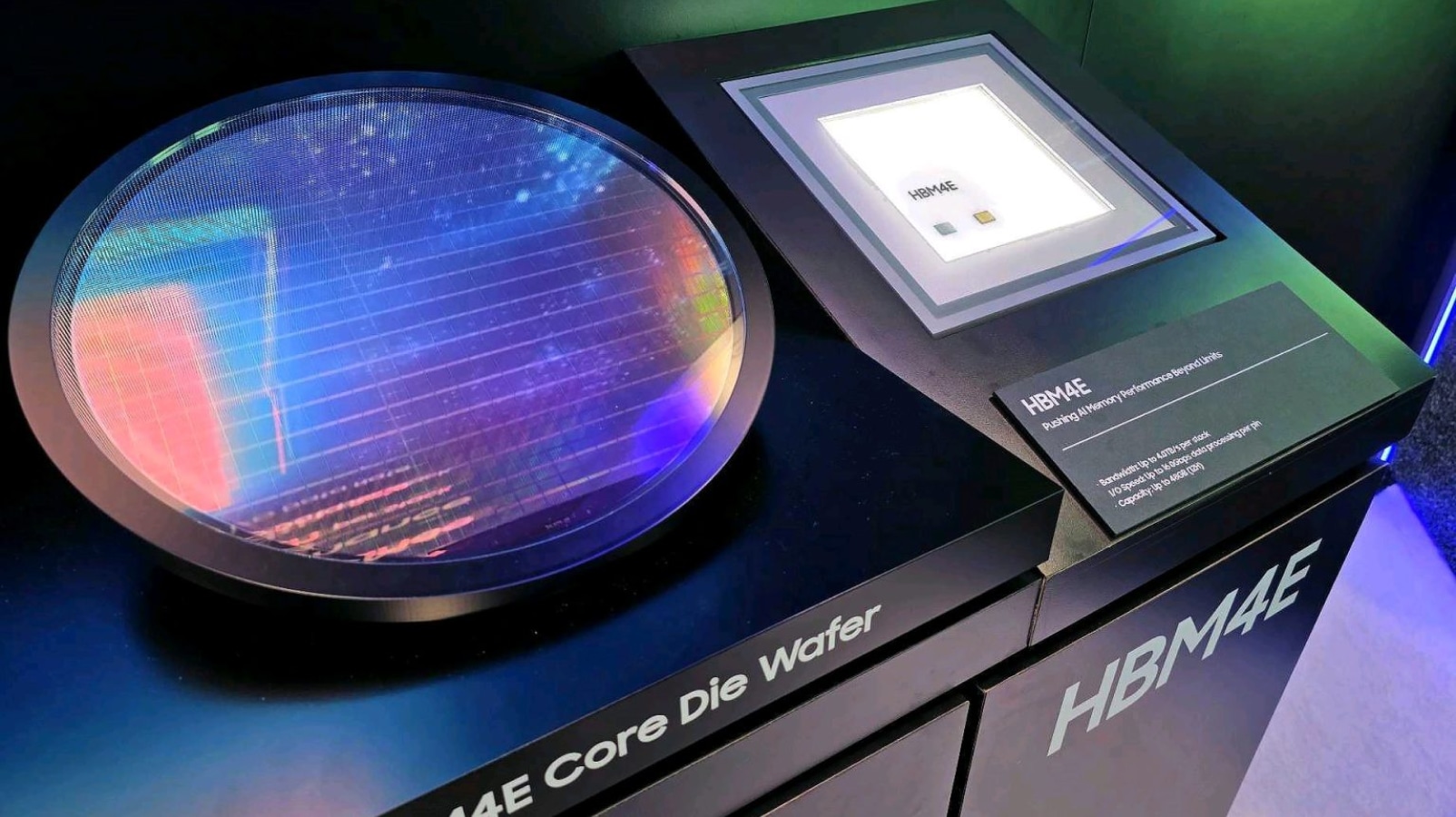
Samsung is developing an 8-layer HBM4E stack for Nvidia’s customized NVHBM requirements.
Why It Matters
If Samsung meets Nvidia’s speed and qualification requirements, it could become a more important supplier for AI accelerator memory. The shift toward an 8-layer design may also show that performance, thermal constraints, and packaging practicality are being balanced against maximum stack capacity.
What To Do Next
Ask your GPU and server vendors whether upcoming Nvidia platforms require 17–18 Gbps HBM4E, then update capacity, bandwidth, and procurement assumptions accordingly.
Key Points
- •Samsung is developing an 8-layer HBM4E stack for Nvidia’s customized NVHBM requirements.
- •The design reduces the planned stack height from earlier 12-layer and 16-layer versions.
- •Nvidia’s target speed is 17–18 Gbps, exceeding Samsung’s initial 14.4 Gbps samples by about 20%.
🧠 Deep Insight
Background and context from public sources — not the original article. 11 sources cited.
🔑 Enhanced Key Takeaways
- •Samsung is specifically targeting the Rubin Ultra AI GPU architecture, which is scheduled for a 2027 market launch.
- •The shift to an 8-layer configuration is primarily driven by the need for improved thermal management and higher manufacturing yields compared to the more complex 12-layer and 16-layer stacks.
- •Samsung leverages a 'turnkey' manufacturing advantage by producing both the DRAM components and the logic-based base dies in-house, unlike competitors who may rely on external foundries for base die logic.
- •The NVHBM platform integrates the memory controller directly into the HBM base die, a design choice intended to maximize power efficiency and bandwidth for NVIDIA's custom AI workloads.
- •Samsung has been diversifying its AI memory strategy beyond HBM4E, including the development of LPDDR5X-PIM (Processing-in-Memory) and High Bandwidth Compute (HBC) architectures.
📊 Competitor Analysis▸ Show
| Feature | Samsung (HBM4E) | SK Hynix (HBM4E) | Micron (HBM4E) |
|---|---|---|---|
| Base Die Logic | In-house (Turnkey) | External Foundry | External Foundry |
| Stack Focus | 8-layer (Thermal/Yield) | 12/16-layer (Capacity) | 12-layer (Capacity) |
| Target Speed | 17–18 Gbps | 16–17 Gbps (est) | 16 Gbps (est) |
🛠️ Technical Deep Dive
- NVHBM Architecture: Integrates the memory controller directly into the HBM base die to reduce latency and improve power efficiency.
- Thermal Management: 8-layer stack height reduction facilitates better heat dissipation compared to 12-layer or 16-layer alternatives.
- Manufacturing Process: Utilizes Samsung's proprietary in-house logic-based base die production to maintain supply chain control.
- Performance Metrics: Targets 17-18 Gbps per pin, representing a 20% performance increase over initial 14.4 Gbps HBM4E samples.
🔮 Future ImplicationsAI analysis grounded in cited sources
⏳ Timeline
📎 Sources (11)
Factual claims are grounded in the sources below. Forward-looking analysis is AI-generated interpretation.
Weekly AI Recap
Read this week's curated digest of top AI events →
👉Related Updates


AI-curated news aggregator. All content rights belong to original publishers.
Original source: cnBeta (Full RSS) ↗
This is a summary, not the original. Read the source, or get the weekly briefing.
Weekly AI briefing
One email a week. Unsubscribe anytime.