Samsung Sets Record R&D Spending
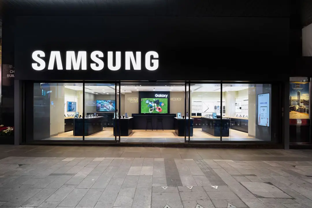
💡Samsung’s record R&D budget may shape the next wave of AI chips and memory supply.
⚡ 30-Second TL;DR
What Changed
First-half 2026 R&D spending reached 27.3 trillion Korean won.
Why It Matters
The record investment could strengthen Samsung’s long-term competitiveness in semiconductors, memory, devices, and AI-related infrastructure. AI builders should watch for future announcements involving advanced memory, chips, and computing platforms.
What To Do Next
Monitor Samsung’s semiconductor and memory product announcements before selecting hardware suppliers for new AI inference or training deployments.
Key Points
- •First-half 2026 R&D spending reached 27.3 trillion Korean won.
- •Spending increased 51.5% from 18.06 trillion Korean won a year earlier.
- •The investment represents Samsung Electronics’ highest first-half R&D expenditure on record.
🧠 Deep Insight
AI-generated analysis for this event.
🔑 Enhanced Key Takeaways
- •The surge in R&D spending is primarily driven by Samsung's aggressive push into next-generation semiconductor manufacturing, specifically 2nm and sub-2nm gate-all-around (GAA) process technologies.
- •A significant portion of the capital is being allocated to the 'Samsung Advanced Institute of Technology' (SAIT) to accelerate breakthroughs in generative AI hardware and neuromorphic computing architectures.
- •Samsung has increased its investment in high-bandwidth memory (HBM4) development to maintain competitiveness against SK Hynix in the AI accelerator supply chain.
- •The company is expanding its R&D footprint in North America and Europe to secure top-tier talent in AI software and system-on-chip (SoC) design.
- •Despite the record R&D expenditure, Samsung's operating profit margins remain under pressure due to the high cost of extreme ultraviolet (EUV) lithography equipment and cleanroom facility expansions.
📊 Competitor Analysis▸ Show
| Feature/Metric | Samsung Electronics | TSMC | Intel | SK Hynix |
|---|---|---|---|---|
| Primary Focus | Memory/Logic/Foundry | Pure-play Foundry | IDM 2.0/Foundry | Memory (HBM) |
| R&D Strategy | Vertical Integration | Process Leadership | Fab Expansion | AI Memory Specialization |
| GAA Capability | 3nm/2nm (Active) | 2nm (Planned) | 18A (In Progress) | N/A |
🛠️ Technical Deep Dive
- Focus on Gate-All-Around (GAA) transistor architecture to improve power efficiency and performance at the 2nm node.
- Development of HBM4 (High Bandwidth Memory) utilizing advanced packaging techniques like hybrid bonding to increase data transfer rates for AI workloads.
- Integration of AI-driven design automation tools to reduce the time-to-market for custom SoC designs.
- Research into backside power delivery networks (BSPDN) to mitigate voltage drop and improve signal integrity in advanced logic chips.
🔮 Future ImplicationsAI analysis grounded in cited sources
⏳ Timeline
Weekly AI Recap
Read this week's curated digest of top AI events →
👉Related Updates


AI-curated news aggregator. All content rights belong to original publishers.
Original source: cnBeta (Full RSS) ↗