🇨🇳cnBeta (Full RSS)•Freshcollected in 5h
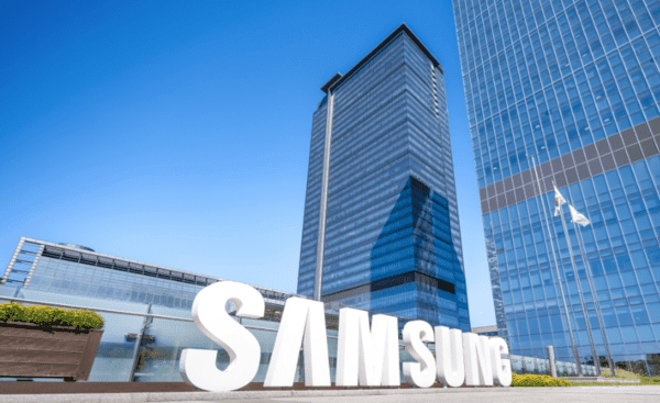
Samsung secures major Meta ASIC order for AI chips
💡Major shift in AI hardware supply chain as Meta moves ASIC production to Samsung.
⚡ 30-Second TL;DR
What Changed
Samsung wins major ASIC manufacturing contract from Meta.
Why It Matters
This move intensifies the competition in the AI semiconductor foundry market, potentially diversifying supply chains away from TSMC for major AI developers.
What To Do Next
Monitor Samsung's process node availability for custom ASIC development if you are planning large-scale AI infrastructure deployments.
Who should care:Enterprise & Security Teams
🧠 Deep Insight
AI-generated analysis for this event.
🔑 Enhanced Key Takeaways
- •The Meta ASIC order is reportedly utilizing Samsung's advanced 2nm (SF2) gate-all-around (GAA) process technology, marking a critical test for Samsung's yield rates against TSMC.
- •This partnership signifies Meta's strategic move to diversify its supply chain away from exclusive reliance on TSMC for its custom silicon, specifically for its MTIA (Meta Training and Inference Accelerator) roadmap.
- •Samsung's foundry division has integrated its 'Advanced Packaging' (AVP) business unit to provide turnkey solutions, including HBM4 integration, which was a decisive factor in winning the Meta contract.
- •The 50 trillion KRW backlog is largely driven by long-term supply agreements (LTSAs) with hyperscalers, which include clauses for capacity reservation and co-investment in cleanroom infrastructure.
- •Industry analysts note that this deal includes a 'yield-guarantee' incentive structure, where Samsung assumes a portion of the financial risk if production yields do not meet specific performance-per-watt targets for Meta's AI clusters.
📊 Competitor Analysis▸ Show
| Feature | Samsung Foundry | TSMC | Intel Foundry |
|---|---|---|---|
| Leading Node | 2nm (SF2) GAA | 2nm (N2) GAA | 18A (RibbonFET) |
| Packaging | I-Cube / H-Cube | CoWoS | Foveros |
| AI Focus | Turnkey (Logic + HBM) | High-volume Logic | System Foundry |
| Pricing | Aggressive/Incentivized | Premium/Market Leader | Competitive/Entry |
🛠️ Technical Deep Dive
- The Meta ASIC is expected to leverage Samsung's SF2 (2nm) process, which utilizes Multi-Bridge-Channel FET (MBCFET) architecture to improve power efficiency by approximately 25% compared to 3nm nodes.
- Implementation involves the integration of HBM4 memory via 2.5D/3D packaging, utilizing Samsung's AVP (Advanced Packaging) capabilities to manage the high thermal density of Meta's inference workloads.
- The chip architecture is optimized for Transformer-based models, specifically focusing on FP8 and INT8 precision arithmetic to accelerate LLM inference tasks.
- The design utilizes a chiplet-based architecture, allowing Meta to scale compute resources by interconnecting multiple ASIC dies on a single interposer.
🔮 Future ImplicationsAI analysis grounded in cited sources
Samsung's 2nm yield will determine its long-term viability as a Tier-1 AI chip manufacturer.
If Samsung fails to achieve competitive yields on the Meta order, it risks losing future high-volume contracts to TSMC's more mature 2nm process.
Meta will reduce its dependence on NVIDIA GPUs by 2027.
The successful deployment of custom ASICs manufactured by Samsung allows Meta to shift inference workloads to internal hardware, lowering total cost of ownership.
⏳ Timeline
2022-06
Samsung begins mass production of 3nm GAA process, the first in the industry.
2023-05
Meta announces the first generation of its custom MTIA chip for AI inference.
2024-04
Meta unveils the next-generation MTIA chip, signaling a shift toward internal silicon development.
2025-02
Samsung announces the expansion of its AVP (Advanced Packaging) business unit to support AI chip demand.
2026-01
Samsung reports record-high foundry backlog exceeding 45 trillion KRW.
📰
Weekly AI Recap
Read this week's curated digest of top AI events →
👉Related Updates


AI-curated news aggregator. All content rights belong to original publishers.
Original source: cnBeta (Full RSS) ↗