Samsung Labor Strike Risks Global AI Supply Chain
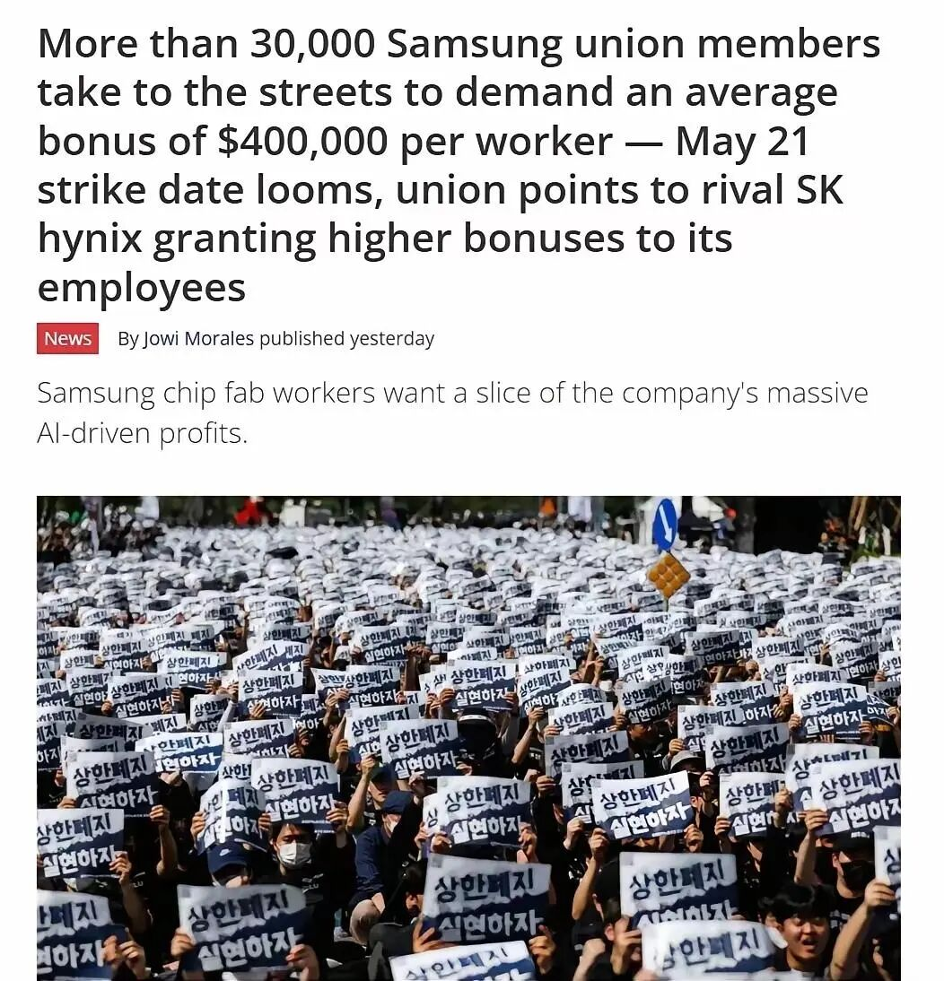
💡Understand how labor disputes at major memory suppliers can create bottlenecks for your AI infrastructure projects.
⚡ 30-Second TL;DR
What Changed
Samsung produces 40% of global DRAM and 30% of NAND, making its stability critical for AI hardware.
Why It Matters
The incident underscores the extreme reliance of the AI industry on a few memory manufacturers. Future supply chain strategies must account for geopolitical and labor risks in the semiconductor sector.
What To Do Next
Diversify your hardware procurement strategy and monitor HBM supply lead times to mitigate risks from single-source dependency.
Key Points
- •Samsung produces 40% of global DRAM and 30% of NAND, making its stability critical for AI hardware.
- •The strike specifically threatened HBM production, a key component for AI accelerators like NVIDIA's GPUs.
- •Market concentration in the memory sector means supply chain shocks are amplified for AI data centers.
- •Legal intervention classified Samsung's semiconductor plants as 'safety facilities' to prevent production halts.
🧠 Deep Insight
Background and context from public sources — not the original article. 23 sources cited.
🔑 Enhanced Key Takeaways
- •The recent labor agreement, approved on May 27, 2026, resolved the immediate strike threat but caused significant internal conflict within Samsung due to a large disparity in performance bonuses between the profitable semiconductor (DS) division and other divisions like finished products (DX).
- •A court injunction issued on May 18, 2026, legally restricted the strike's impact by mandating the continuation of essential semiconductor production and maintenance, preventing a complete shutdown of facilities.
- •Samsung's first-ever majority union, the Trans-Company Union, lost its majority status on June 4, 2026, after approximately 18,000 members defected, largely due to dissatisfaction with the wage agreement's bonus structure favoring the semiconductor division.
- •Despite recent challenges in HBM market share, Samsung plans to significantly boost its HBM production capacity by about 50% in 2026, aiming for 250,000 wafers per month by year-end, with a strong focus on HBM4.
- •The broader HBM market is characterized by an oligopoly of SK Hynix, Micron, and Samsung, with SK Hynix currently holding the largest share (62% as of Q2 2025), and all three suppliers having their 2026 HBM capacity largely sold out to hyperscalers.
📊 Competitor Analysis▸ Show
| Feature/Metric | Samsung Electronics | SK Hynix | Micron Technology |
|---|---|---|---|
| HBM Market Share (Q2 2025) | 17% | 62% | 21% |
| HBM3E Status | Completed validation in 2025, mass production ramping | Dominant position, early and exclusive supply agreements with NVIDIA | Shipping 12-stack HBM3E |
| HBM4 Status | Began sampling in 2025, mass production ramping in 2026, first supplier of HBM4 to NVIDIA | Began sampling in 2025, mass production ramping in 2026, preparing for HBM4 market emergence | Began sampling in 2025, mass production ramping in 2026 |
| 2026 HBM Capacity | Plans 50% surge to ~250,000 wafers/month by end of 2026 | Capacity reportedly fully booked for next three years | Entire 2026 production reportedly sold out |
| DRAM Market Share (Q1 2026) | 38% (led market) | 29% | Not specified in Q1 2026, but a major player |
🛠️ Technical Deep Dive
- HBM Fundamentals: High Bandwidth Memory (HBM) is a 3D-stacked DRAM architecture that maximizes data throughput while minimizing power consumption and footprint. It achieves this through Through-Silicon Vias (TSVs) for vertical interconnects and wide I/O interfaces.
- HBM3E (Fifth Generation): This is the current production-grade HBM, delivering over 1.2 TB/s per stack through a 1024-bit wide interface and 16 independent channels. It pushes per-pin data rates beyond 9 Gbps, with capacities up to 36GB per stack.
- HBM4 (Sixth Generation): Defined by JEDEC JESD270-4 (published December 2024, official spec April 2025), HBM4 doubles the interface width to 2048 bits and 32 independent channels. It targets over 2.0 TB/s (up to 3.3 TB/s in advanced configurations) per stack and up to 64GB capacity per stack (via 16-high configurations with 32Gb layers).
- Power Efficiency: HBM4 reduces the core DRAM voltage to 1.05V (from 1.1V in HBM3/3E), contributing to improved power efficiency.
- Architectural Shift: HBM4 is not an incremental speed bump but a redesign of the memory interface and a shift in memory architecture, integrating a logic die and requiring significant redesign of silicon interposers due to the doubled bus width.
🔮 Future ImplicationsAI analysis grounded in cited sources
⏳ Timeline
📎 Sources (23)
Factual claims are grounded in the sources below. Forward-looking analysis is AI-generated interpretation.
Weekly AI Recap
Read this week's curated digest of top AI events →
👉Related Updates


AI-curated news aggregator. All content rights belong to original publishers.
Original source: 虎嗅 ↗
This is a summary, not the original. Read the source, or get the weekly briefing.
The weekly digest
One email a week. Unsubscribe anytime.